
We have heard about the numerous benefits that an FPGA promises. Let us see how exactly these promises are delivered and help decide whether they are savvy enough to suit your project.
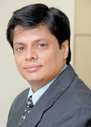
Neeraj Varma, director – sales, Xilinx India, spoke to Anagha P of EFY
Q. Should an engineer be looking at a specific kind of FPGA for a specific application?
A. Field-programmable gate arrays (FPGAs) are not made specific to a market—they are not customised for any particular application at all. Let us say we have a chip that can be used by a medical customer; the same chip could also be used by a defence/military customer or even by a telecom (both wired and wireless) customer. Other fields covered are industrial networking, automotive, broadcast, and high-end consumers.
Q. What are ‘ASIC-class’ FPGAs? What design problems are solved when an FPGA becomes ASIC-class, and how?
A. The whole belief is that the FPGAs in the latest Ultrascale generation have a lot more features that are ASIC-like. First of all, the key here is the ASIC-like class architecture. There are several changes we made in the architecture that are like ASIC, for example, ASICs are always good in power and performance. FPGAs traditionally have an overhead, but we are trying to bridge this gap and did quite well in 28nm, but in 20nm we are going to do even better.
Earlier what we had were very few global clocks. As the density grew, clock skew problem increased. So now we have added more clocking regions, we have more clocking resources placed at different areas of the chip. This is how exactly it is done in ASICs to solve skew problem, and that is why we call it ASIC-class clocking.

Q. What are the three biggest design challenges that an engineer could face while working with last-gen FPGA chips?
A. Imagine you have data files running at 10Gb per data versus 100Gb per second data versus 400Gb per second data. This data coming inside the FPGAs creates a lot of red areas, which represents straining inside the FPGA.
The biggest problem is, you have a lot of logic that needs to be placed, but to interconnect them you need a lot of routing resources, lot of metal lines. These get strained because your clock period is going down and bus width is going up. So you have a huge amount of data, very large buses, and this strains your interconnect. Because it is so large, there would be two types of delays; a delay between when the signal goes in and the signal goes out, and the second one is the routing delay. A routing delay becomes a lot more pronounced inside the chip, at sub-micron level.
The second problem is clock skew. If the chip is bigger, the clock at one point versus other point has a skew. Third problem in traditional FPGA design is that the usage of configurable logic blocks (CLBs) is not optimal.
Q. How are these problems solved?
A. As the number of logic cells are increasing, we are increasing the routing resources. Essentially it was only vertical and horizontal. Now we are adding lines which can connect different blocks on a different scale. The problem of clock skew was, earlier we had just one global clock which provided clock signal to the entire chip, which produced a skew. But just like in ASIC, we now have a lot more clocking resources across the chip and this helps manage the skew. Finally, the tools are doing a better job in packing.
Q. What is one exciting development on the design tool side for FPGAs?
A. The other thing that we have introduced is high-level synthesis (HLS). Traditionally, people have been designing ASICs and FPGAs with HDL and Verilog. HLS allows people to write C, C++ programs and convert those into HDL. So you do not really need an army of HDL designers to design an FPGA. Even software engineers can now design with FPGA. This is a big productivity boost for customers, as many people know C, but not VHDL.
Q. What is the scale of improvement when you compare the last two generations of FPGAs?
A. The density of logic cells has increased by almost four times that of the Virtex-7 series. In terms of performance, we have changed the architecture significantly and we are able to get at least 30-40 per cent performance improvement. Due to the adoption of FinFET technology, and other architectural and tool enhancements, the power consumption of the device has come down by 30-40 per cent. The bill of materials (BOMs) cost for customers has also reduced significantly. Productivity has increased as well. We are now promising more than 90 per cent utilisation of the device.


