Automated test equipment saves cost and enhances efficiency for product manufacturers. Let us see out what drives the most popular automated test equipment used in the industry
Pankaj V.
Testing has always been a vital part of manufacturing industries, but rapid advancements at Silicon Valley have resulted in a highly competitive market. This has driven the need for reduction in the product development cycles, and at the same time ensuring product reliability and quality, which makes it even more impactful. The speed and effectiveness of product testing have a significant impact on quality assurance and time to market for the products.
Automated test equipment (ATE) contributes towards product success by providing swift and reliable testing and monitoring solutions. There are a variety of ATEs being used in the electronics industry today, each having a different approach for the testing and measurement.
Automated optical inspection
One of the efficient testing solutions for today’s small, compact and complex electronics is automated optical inspection (AOI). It is a non-contact test method for automated visual inspection, which can be used for the detection of a variety of surface defects in PCBs.

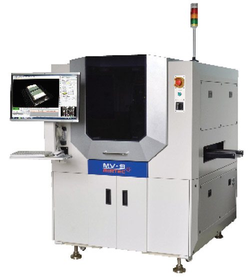
How does it work? AOI system scans the board with high-definition cameras and then processes the captured images for analysis and inspection of defects. Imaging systems are the heart of the AOI systems. Today we have more flexible and scalable imaging sensors—best suited for the high-end microelectronics. Strobed inspection modules for image acquisition have also contributed to better imaging sensor resolution, resulting in an increased speed and accuracy of the AOI systems. Introduction of 3D AOIs has simplified the inspection of SMT devices on finished PCB assemblies, yielding precise height measurements for the correct detection of lifted components and lifted lead defects along with the solder volume post reflow.
Rajeev Kaushal, general manager-PES, eInfochips, explains, “To improve performance in terms of speed and accuracy, algorithms are optimised and ported on DSP/FPGA platforms to carry out online AOI. To avoid computational complexities, the lighting and locational parameters are controlled, which results into minimal use of pre-processing algorithms, hence improvement in execution. Experience-based new logics are also designed and implemented on platforms for specific AOI applications. It has improved accuracy tremendously and the platforms are integrated with external systems for faster response and action. The new AOI platforms also support integration of multiple sensors that cater to the needs beyond optical inspection and include thermal inspection also.”
Most AOI systems’ lighting requirements depend upon the type of defects, product and distance from the camera. The positioning of lighting as well as type of light source is also very important, shares Rajeev. Ideally, full surface should be uniformly lit without shadow, shine or any artefacts because of lighting. Different types of lighting are available:
1. Fluorescent lighting. Thoug widely used for PCB AOI, the main problem with fluorescent lighting is that the lamps degrade with time. This means that the AOI system will be subject to constantly changing levels and quality of light.
2. LED lighting. LED lighting is very well received for AOI applications, as level of lighting can be controlled and it does not degrade.
3. Infrared or ultraviolet. Required for specific applications.
Trends in AOI. The component size and power consumption are extremely important factors in AOI as they help in mobility as well as maintenance. “Trend is towards miniaturisation of components and compact AOI machines. Application-based right type of sensors, platform with proper connectivity and integrated sensors with smaller size and ease of use are limited in market. The market is growing and near threshold. Once it crosses the threshold (say 2-3 years from now), availability of platforms, components, integration and services would not be a challenge,” explains Rajeev.
Automated X-ray inspection
Automated X-ray inspection (AXI) systems are almost similar to AOI systems and are also used for PCB inspection. High-density ICs and BGAs (ball grid arrays) are difficult to test with AOI systems as they have connections underneath the packages. AXI systems use X-rays instead of visible light and thus are able to inspect the elements that are not visible to AOI systems.
High-focus systems with sub-micron spot sizes are ideal for the MEMS, opto-electronics, mobile phones, telecom electronics, BGAs and loaded PCBs. 3D imaging has increased AXI performance manyfold, as AXIs are having angled 3D imaging with optional computed tomography (CT) system for reconstruction of 3D images to gain more insight into components and sub-assemblies. Higher magnification for zooming in on specific areas with user-friendly software adds to the AXI testing ranges.
In-circuit testing
In-circuit testing (ICT) is a comprehensive PCB testing technique, which measures circuit parameters such as resistance and capacitance, along with the operation of analogue components such as operational amplifiers and some functionality of digital circuits.