
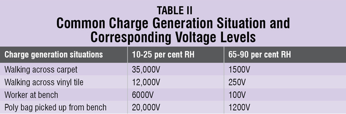
When an electrostatically-charged person or object touches an ESD-sensitive device, there is a possibility of the electrostatic charge being drained through sensitive circuitry in the device. If the ESD possesses sufficient energy, damage could occur to the device due to localised overheating. Generally, devices with finer geometries are more susceptible to damage from ESD. The common sources of static charge in a lab are mentioned in Table III.


Electrostatic induction. This is another phenomenon responsible for static charge build up. It occurs when an electrically charged object comes near a conductive object isolated from the ground. The charged object produces an electrostatic field that causes electrical charges on the surface of the other object to redistribute as shown in Fig. 2. As such, the net charge on the object will be zero, but it will have surfaces with excess positive and negative charge and so an ESD event can happen from those surfaces.
Classification of ESD sensitivity
It is important to define ESD sensitivity level of various components and products. These are commonly characterised to three defined models:
1. Human body model (HBM)
2. Machine model (MM)
3. Charged device model (CDM)
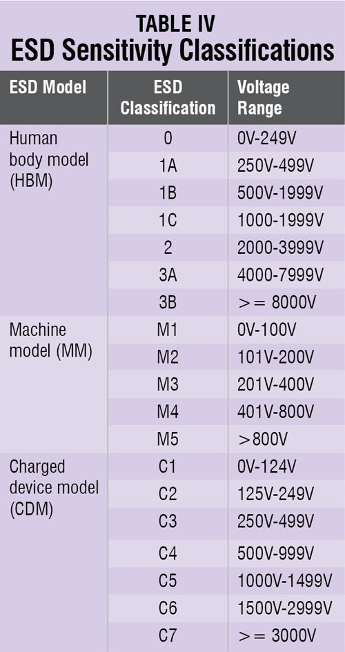 ANSI/ESD S20.20 defines a control program for items that are sensitive to 100V human body model. The procedures in ANSI/ESD S20.20 may need to be tailored or expanded in specific situations. Based on the models used, the ESD-sensitive parts can be classified in accordance with Table IV. It should be noted that the HBM, MM and CDM voltage levels do not correlate with each other.

Here an important question arises: How do we determine the sensitivity of our parts and assemblies, or where can we get this information?
The first source would be the manufacturer or supplier of the component itself or the part data sheet. An additional source could be an organisation like System Reliability Center in Rome, which publishes ESD susceptibility data for 22,000 devices, including microcircuits. This data is very generic and may not specifically cover the part you are actually using, but it can give a very good idea about the approximate levels.
ESD control
Now that we have discussed the cause of ESD, let us see how we can control it. To have good ESD control, we first need to identify the problem areas very carefully.
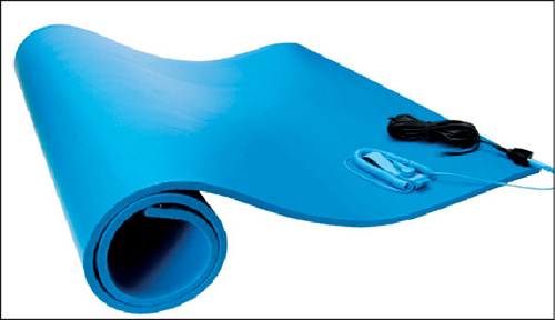
The work area should be marked as electrostatic protective area (EPA) and you should only be handling ESD-sensitive components within this area. This area needs to be protected by proper ESD grounding of the workers, equipment and work surfaces.
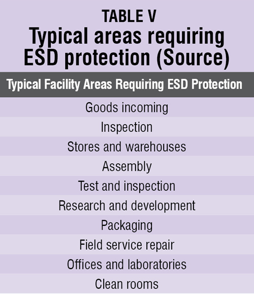
Problem area. Table V shows typical areas which need special attention for ESD control. Each electronic component goes through various levels during the manufacturing process, so it is important that ESD control is implemented everywhere. Otherwise, damage could be caused at any stage.
 There are basically two categories of damage from ESD.
The first is catastrophic damage where the electronic device is inoperable immediately after the ESD event. A semiconductor junction or a connecting metallisation could have been damaged by the ESD.
The second is latent damage where the electronic device appears to be working fine following the ESD event but the sensitive circuitry has been damaged and could fail to operate properly at some time in the future.
Grounding
The static charge generated due to tribocharging and electromagnetic induction flows from higher to lower potential causing ESD events. The only way to control ESD events is by grounding all the generated charge as quickly as possible with the ESD common ground. All conductors and dissipative materials in the environment, including workers, must be bonded or electrically connected to this ground.
Now the ESD common ground should be connected to electrical ground connection as recommended in ANSI/ESD S6.1-Grounding standard. This is a good practice as all electrical equipment at the workstation is already connected to this ground. Connecting the ESD control materials or equipment to the electrical ground brings all components of the workstation to the same electrical potential.
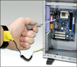


Personal grounding. Grounding works very efficiently in ESD control systems and reliably removes electrostatic charges to ground. For such a grounding system, it is important that electrical wiring system of your lab is correct.
Electrical outlets need to be checked to verify the correct wiring of live, neutral and ground. Wrist straps are the most common way of personal grounding. Clothes are proven to be a conductor of ESD charges, therefore ESD garments are a good idea for added protection. The basic ESD garments used in the electronics industry are ESD aprons, gloves and shoe-covers.