


- User I/O: Papilio-style wing interface with 48 user-defined I/O signals. The boards have female headers installed on the wing interface.
Other than the ones mentioned above, the market is full of other popular boards for Spartan-6, such as XuLA2, 5I25 from Mesa Electronics, Numato Mimas, Numato Saturn and many more. XuLA2 has an LX25 chip on a small breadboardable PCB with built-in USB programmer, 32MB RAM, 8Mb Flash, 33 I/Os and SD card socket. The design is completely open source.
Mesa Electronics has a slightly baffling array of FPGA boards. Two interesting ones are 5I25, which is a PCI card with a Spartan-6 LX9, and 6I25 (PCI Express).
Numato Mimas provides a Spartan-6 LX9, 16Mb Flash, 100MHz oscillator, USB programming interface, eight LEDs, four switches and 70 I/Os.

Numato Saturn provides a Spartan-6 LX9, LX16, LX25 or LX45, 16Mb Flash, 100MHz oscillator, 512Mb LPDDR RAM, USB programming interface and GPIOs (via the FT2232H) and 118-150 I/Os.
Artix-7
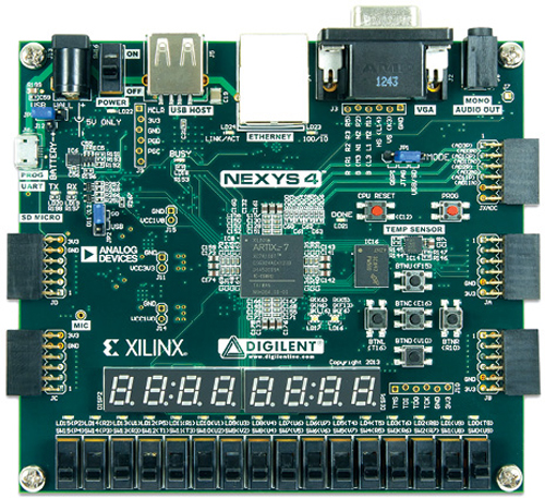
1. Nexys-4
- 15,850 logic slices, each with four 6-input LUTs and eight flip-flops
- 4860 kbits of fast block RAM
- Six clock management tiles, each with phase-locked loop (PLL)
- 240 DSP slices
- Internal clock speeds exceeding 450MHz
- On-chip analogue-to-digital converter (XADC)
- 16 user switches, 16 user LEDs and two 4-digit seven-segment displays
- USB-UART bridge, 10/100 Ethernet PHY and 12-bit VGA output
- On-board 3-axis accelerometer, temperature sensor
- PWM audio output and PDM microphone
- Micro-SD card connector
- Digilent USB-JTAG port for FPGA programming and communication
Development boards for Lattice chips
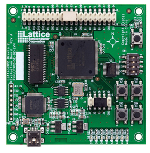
1. Lattice XP2 Brevia
- LatticeXP2 FPGA: LFXP2-5E-6TN144C
- 2Mb SPI Flash memory
- 1Mb SRAM
- On-board USB controller for JTAG programming (FTDI -FT2232H)
- 2×20 and 2×5 expansion headers
- Push-buttons for GPIO and reset
- 4-bit DIP switch for user-defined inputs
- Eight status LEDs for user-defined outputs
LatticeXP2 Brevia is a development board with a small problem—the programmer needs a parallel port, and the USB programming cable is sold separately. The FPGA is a pretty low-end part as compared to the XC3S500E.
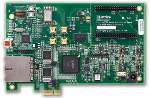
2. LatticeECP3 Versa
- LatticeECP3 FPGA: LFE3-35EA-8FN484C
- 64Mbit SPI Flash memory
- 1Gbit DDR3
- PCI Express x1 interface
- Four SMA connectors for electrical testing of one full-duplex SERDES channel
- Two RJ45 interfaces to 10/100/1000 Ethernet to GMII
- Expansion connectors for prototyping
- 14-segment alphanumeric display
- Switches, LEDs and displays for demo purposes
- Push-buttons for GPIO and reset, on-board reference clock sources
- Programmed using a mini-USB cable via PCROHS-compliant
LatticeECP3 Versa is one of the cheapest PCI-Express development boards so far. It also has two gigabit Ethernet ports and high-speed serial connectors. It appears that the FPGA device requires a licenced version of the design software.
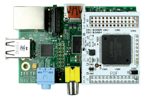
3. Bugblat pif
- A complete FPGA development target—FPGA programming hardware is not needed
- Plenty of on-chip 4-input LUTs—the pif-1200 has 1280, the pif-7000 has 6864
- Plenty of on-chip 9kbit SRAM blocks—the pif-1200 has 7, the pif-7000 has 26
- The FPGA is nonvolatile, with on-chip Flash memory for storing the configuration bit stream
- Up to 256kbits user Flash memory
- Hard-coded I2C, SPI, PLL and timer/counter blocks
- Powered from the Raspberry Pi expansion connector (P1)
- 47 pins of expansion connectors
- Red and green LEDs
- Support software supplied (in Python) for injecting a new configuration into the FPGA
- Example projects supplied, including a project that controls logic inside the FPGA from a web browser
Bugblat pif is a Raspberry Pi add-on board that provides a MachXO2-1200 or -7000, 17 external I/Os (in addition to those used to communicate with the Raspberry Pi), two LEDs and programming circuitry.
The other popular development boards for Lattice FPGAs are iCEblink40-HX1K Evaluation Kit, TRIFDEV and Bugblat tif.
iCEblink40-HX1K Evaluation Kit comes with a USB programmer, four LEDs, four capacitive touch buttons, configuration PROM, 68 digital I/Os and supposedly some PMOD and Arduino shield compatibility.
TRIFDEV is an Arduino shield that provides 58 extra I/Os, and can also be used as a standalone development board. It has a MachXO2-1200, USB programmer, two buttons and five LEDs.
Bugblat tif is a coin-sized, breadboardable MachXO2-1200 or -4000 board. It has ten I/Os, USB programming (with cross-platform open source software that does not require drivers) and two LEDs.
