Wide Bandgap – The material of the future?
Managing and using power efficiently is one of the challenges of modern times. Power is a common theme in almost every electronic design and is becoming increasingly common in vehicles, to store the incredible amount of data we produce, harvesting energy from nature and also in every small portable device we use to help us manage our busy daily lives.
At the heart of any power solution is a semiconductor switching device. Conventionally, these have been made from silicon, yet these have reached a point where further efficiency gains are unlikely and other materials are being explored. So-called wide bandgap (WBG) materials are emerging that can increase the efficiency of DC/DC converters from 85% to around 95%, or DC/AC inverters can go from 96% to 99% – clearly a significant improvement.
Gallium nitride (GaN) is one of the first WBG materials to become commercially available and is commonly used in high electron mobility transistors (HEMT). When compared with silicon-based superjunction transistors, GaN-based HEMT offer much lower switching losses due to their lower input and output capacitances (Ciss and Coss). Switching speeds are also faster, mainly due to the lower Miller capacitance which means that higher frequency topologies can be used, thereby reducing the size, weight and cost of components, especially magnetic devices. GaN also exhibits a lower on-resistance per die area than silicon, reducing static losses and lowering heat generation from the device. As a result, devices can be smaller and the cost and size of thermal management (such as heatsinks or fans) can be reduced, further reducing the system size and cost.

Commercial availability of GaN
Until now, the availability and adoption of GaN has been relatively limited. In part, this is due to the silicon-based superjunction transistor that has extended the figure-of-merit to a point where acceptable performance is achievable. The other factor, and possibly the most important, has been the high cost of these devices, linked to the low sales volumes.
The situation is changing. As users demand ever-higher performance and efficiency from power supplies, designers have little alternative but to embrace GaN technology. As a result of the greater usage, and some further development of the technology, the economies of scale are beginning to make these devices more economically viable – which will lead to greater adoption and further cost reductions.
There are two primary types of GaN power transistor; the normally-on depletion-mode devices that require a negative gate voltage (relative to the drain and source potential) to turn off and the normally-off enhancement-mode (e-mode) devices that require a positive gate voltage to turn on.
One area for careful consideration, especially with depletion-mode GaN FETs, is the start-up phase. In a half-bridge topology both the upper and lower switches would normally be on creating a short circuit, so the gate control circuits must be started first to apply a negative bias to the GaN FETs to avoid powering up into a short circuit.
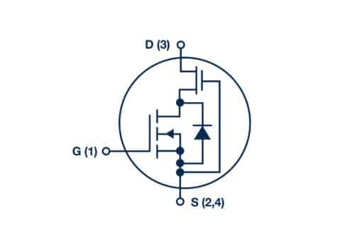
Alternatively, depletion-mode GaN transistors can be used with a low-voltage silicon MOSFET in cascode configuration. In this arrangement, the GaN transistor source is connected to the silicon MOSFET drain, and the silicon MOSFET source is connected to the GaN transistor gate as shown in Figure 1. When no bias is applied to the silicon MOSFET gate, its drain-source voltage (Vds) negatively biases the GaN transistor gate, to keep the device turned off. GaN FETs are available co-packaged in cascode configuration – one example being the ON Semiconductor NTP8G202NG.
Another way to eliminate start-up short circuits is to use an enhancement-mode GaN HEMT that is normally off. The GaN Systems GS66516B is a 650V device that operates from a low (0-6V) gate voltage, thereby simplifying the design challenge. Despite the low gate voltage, the device tolerates gate transient voltages from -20V to +10V. The device is very suitable for modern power applications, allowing operation at speeds up to 10MHz and providing six contacts in its bottom-side cooled package. The GS66516B can handle drain-source currents up to 10A, while operating efficiently due to it 25mΩ on-resistance.
Design of switching circuits
Designers must ensure that the devices are turned fully on and fully off quickly to ensure proper operation. To achieve this, a well matched and configured gate driver is required, as is common with all power devices. One essential consideration is ensuring that, when turning on, the driver charges the transistor’s gate capacitance quickly with no ringing or overshoot. The same applies to the turn off, where discharging the gate capacitance but also be accomplished cleanly. In bridge configurations, “Shoot through” short circuits are another potential issue – these can be avoided by ensuring the skew time is well controlled and that the performance of the driver is consistent.When designing drive circuits for GaN devices designers must consider the maximum allowable gate voltage, the gate threshold voltage, and the body diode voltage drop. For an enhancement-mode GaN device, such as the GS66516B, the 6V gate-source voltage is half that of a MOSFET, making the generation of the turn-on / turn-off voltages and currents far simpler. The forward-voltage drop of the transistor’s intrinsic body diode is about 1 volt higher than comparable silicon MOSFETs. As the temperature coefficient is lower, compensation circuit requirements are also simpler.
GaN devices are generally faster than MOSFETs with comparable values of RDS(ON). In fact, turn-on times are typically four time faster while turn-off times are twice as fast. At the system level this delivers benefits although additional care is needed dynamic performance of the driver as dV/dt rates can exceed 100V/ns. There is a distinct possibility of creating a shoot-through condition during the transition phase which can affect the efficiency of the system.
Adjusting the gate drive pull-up resistor can achieve the fastest transition time without creating other loss-creating effects. By optimizing this resistance overshoot and ringing are also diminished thereby avoiding false turn-on/ / turn-off and also significantly reducing EMI. To further reduce high-frequency LC-ringing in practical applications designers may wish to add ferrite beads in series with the gate and also consider an RC ‘snubber’ across the gate-source path.
Figures 2 and 3 give a graphical overview of a GaN transistor’s turn-on / turn-off performance and shows the topics to consider for reliable operation.


The turn-on and turn-off performance can be individually optimised for GaN devices with a low threshold voltage by splitting the pull-up / pull-down connections in the driver, thereby permitting the insertion of a discrete resistor.
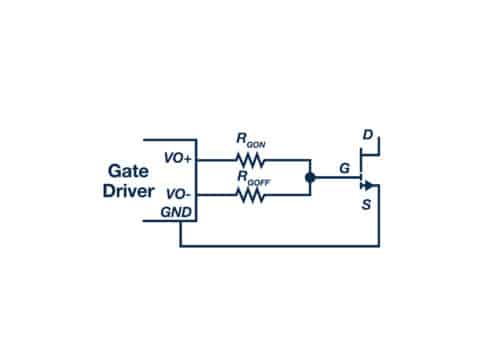
As well as optimizing stability, tweaking the gate turn-on / turn-off resistor ratio will also ensure the highest level of drive performance. A typical value for the turn-on resistor is in the range 10 to 20Ω. Too large a value will reduce the dV/dt slew rate at turn-on, thereby reducing switching speeds and increasing power losses. Gate oscillation and losses from the Miller-effect can be issues if the slew rate is too high. To achieve fast and robust pull-down with minimal impedance the turn-off resistance should be approximately 10% of the turn-on resistance.
Selecting a gate driver
TI’s LMG1205 gate drive IC is designed to address most of the issues that arise when driving GaN devices, while being flexible enough to allow designers to make design adjustments to switching speed and other parameters to suit the selected switching device. The LMG1205 has been optimized for use with enhancement-mode GaN switches and can be used in synchronous buck, boost, or half-bridge topologies where it will drive both the high-side and low-side switches with independent inputs for each side, allowing the ultimate flexibility.
The low propagation delay (typically 35ns) is matched to 1.5ns between channels thereby avoiding shoot-through issues and ensuring high efficiency. The LMG1205 features split-gate outputs to allow the current to be individually optimized and can source 1.2A / sink 5.0A to prevent undesired turn-on during rapid transitions.
There are several comparable devices that were designed specifically for GaN use and are alternatives to the LMG120G. These include the Silicon Labs Si827x series, Analog Devices ADuM4223A/B family and Maxim’s MAX5048C.
However, existing low frequency MOSFET drivers can be used in place of dedicated GaN drivers, provided the performance and features meet the needs of the GaN device.
As well as selecting the correct gate driver and implementing the required drive circuitry, all of the usual considerations for high speed circuits still apply. For example, attention must be paid to the layout, keeping the driver physically close to the switching device to minimize stray and undesired coupling. In some applications a kelvin-source connection can be used to minimize common-source inductance. In other applications there may be a benefit to using power supply rails that are galvanically isolated.
Summary
Wide bangdgap devices such as 600V GaN power transistors are now commercially available, making the performance benefits attainable for all designers. The faster speeds attainable with GaN devices mean that a good understanding of basic high-frequency analog is needed. However, to take full advantage of the new devices, designers have to carefully select the driver IC and ensure that the associated circuitry is designed to ensure proper switching.