Here, we discuss one of the great, open-source circuit and PCB design programs that can help both beginners and professionals in their journey to make quick and precise designs.
Let’s learn how to design circuits and PCBs like a pro with KiCad, the powerful open-source EDA tool. This comprehensive guide covers everything from installation to advanced features like schematic capture, PCB layout, 3D visualization, and SPICE simulation.
Learn tips, shortcuts, and step-by-step workflows to create precise and professional designs for projects of any complexity. Perfect for beginners and experts alike, this tutorial will empower you to build and optimize electronic designs with ease.
Why KiCad?
A good circuit and PCB design is crucial to ensure the success of a product. KiCad EDA is an open-source software tool for electronic design automation (EDA) that helps designers build and validate their designs faster and more efficiently.
KiCAD has emerged over many years as a powerful PCB and circuit design tool with many professional-grade features. It is a cross-platform software that works on Windows, Mac OS, and Linux OS devices.
With this software, it’s pretty easy to do things any design engineer wants. This includes capturing schematics, layouts for PCB, Spice Simulation, generating bill of materials, 3D PCB models, etc. It supports PCBs with up to 32 copper layers and is capable of creating designs of all complexities.
Key Facts
License: Free
Platform: Windows, Linux, Mac OS
Download page: Click here
Home page: Click here
Getting Started with KiCad
After installing KiCAD, you can launch KiCAD by running kicad.exe under Windows and typing ‘kicad’ in the Terminal under Linux. This opens the main window of the KiCad project manager.
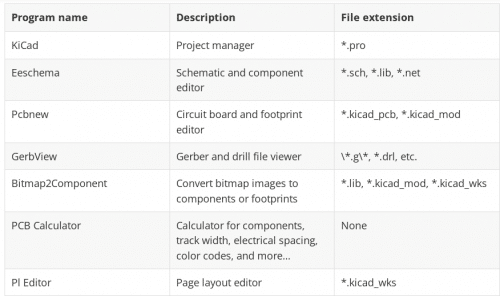
From here you can access the main stand-alone software tools in the KiCAD software suite:
1. KiCad Project Manager
2. EEschema
3. Pcbnew
4. GerbView
5. Bitmap2Component
6. PCB Calculator
7. PI Editor

KiCad Workflow Overview
The typical KiCad workflow majorly consists of two main tasks: schematic creation and board layout. To accomplish these tasks, KiCad includes a vast library of components and PCB footprints and also has the tools to create new ones.
KiCad supports an integrated design workflow in which a schematic and its PCB are designed together. Standalone workflows can be used for special cases.
Any KiCAD project starts with creating the schematics in EEschema, generating PCBs in PcbNew and finally creating Gerber files in GerbView for the manufacturer. Usually, changes are required in the schematics after the PCB layout is done.
You might need to add additional components, use differently sized parts, rename net, etc. You can also make changes in the PCB after the Gerber files are created. Sometimes, there is also a need to create custom parts or footprints for components.
The process of sending schematic information to a corresponding PCB layout is called Forward Annotation. This process is done at least once to import the schematic into the PCB.
Afterwards, forward annotation helps to send incremental schematic changes to the PCB. Backward Annotation is the process of sending a PCB layout change back to its corresponding schematic.
Eeschema, the schematic capture editor features hierarchical sheets, custom symbol creation, and an Electrical rule checker (ERC). PCBnew is the PCB design tool within KiCad.
It is one of the most flexible PCB design software with many modern features such as a design rule checker (DRC) to verify designs, high-speed PCB routing tools such as track-length matching and support for external routing software.
KiCad also comes bundled with additional tools to aid circuit and PCB design, including a PCB calculator to find the values of components or other parameters of a layout, a Gerber viewer to inspect manufacturing files, and an integrated SPICE simulator to inspect circuit behaviour.
KiCad Shortcuts
Accelerator keys and Hotkeys are shortcuts that are both used to speed up working in KiCad by using the keyboard instead of the mouse to change commands.
Accelerator keys have the same effect as clicking on a menu or toolbar icon: the command will be entered but nothing will happen until the left mouse button is clicked. These keys are visible on the right side of all menu panes.
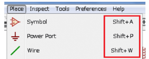
A hotkey is equal to an accelerator key plus a left mouse click. Using a hotkey starts the command immediately at the current cursor location. You can go to Help → List Hotkeys or press Ctrl+F1 to view hotkeys.
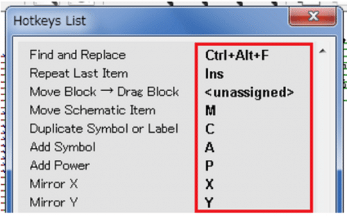
Let’s talk about the tools offered in KiCad in more detail.
Schematic Capture in ‘Eeschema’
Schematic capture involves roughly placing all the components and defining the connections between them on the schematic sheet. Once this is done, a netlist can be generated from the schematic. The schematic netlist is one of the central pieces of information that helps in the creation of a real PCB.
This document provides information on the connectivity of your electronic circuit. They can be used by the manufacturer for design review.
KiCad’s schematic capture software is called EEschema. It is efficient and integrates various essential functions needed for modern schematic capture software. This includes drawing, tracking, creating layouts, access designs of PCB, library management, and more.
You can create a design without any complexity limit. To simplify large and complex designs, you can divide them into hierarchical sub sheets and they can be displayed as single sheets. The interface focuses on productivity.
EEschema is available under the following operating systems: Linux, Apple macOS and Windows, All Eeschema files are 100% compatible from one OS to another, which means that a Linux file will also run on Windows and vice-versa.
You can also export your schematics using a wide range of export options available, including PDF, SVG, HPGL and Postscript.

Features and Highlights:
- Hierarchical schematics: A hierarchical representation helps to manage projects that are bigger than a few sheets. Eeschema manages hierarchical schematics with an integrated “hierarchy navigator” accessible via the icon on the top toolbar. The complete schematic has a main schematic sheet, called a root sheet, and sub-sheets of the hierarchy.
- EEschema is integrated with PCBnew, KiCad’s PCB software to develop PCB designs, and to get info on all the electrical components.
- Symbol library editor: Apart from a vast library of symbols and components, EEschema includes a symbol library editor, with which you can create and edit new symbols and manage libraries.
- Exports netlists in formats such as Pspice, Cadstar, PcbNew and “Generic” XML.
- Bill of Material tool: BOM generation is extensible via Python scripts or XSLT, which allows many configurable formats.
- The electrical rules check (ERC) automatically verifies your schematic connections. It checks for output pin conflicts, missing drivers and unconnected pins.
Layout and Routing
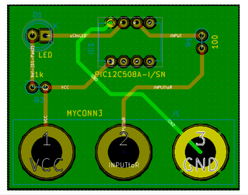
A good PCB layout helps to create a reliable and cost-effective design. PcbNew is KiCad’s layout editor that offers tremendous capabilities. This tool works with EEschema to design and create printed circuit boards.
With PcbNew, you can design PCBs that are very simple to extremely complicated and dense ones. You can make PCB layouts with up to 32 copper layers and additional technical layers.
Routing, the process of defining or placing signal traces according to the schematic, is one of the most important steps in PCB design.
On one hand, manual routing mode offers design flexibility while improving your skills.
On the other hand, auto routers reduce the workload associated with the design of advanced and complex boards. Auto routers follow a set of design rules to automatically route the PCB board.
While designing complex boards, many designers, however, attain a balance where critical components are routed by hand and auto routers are used for the rest of the design.
PcbNew features a simple but effective auto router to assist in the production of the circuit board. An Export/Import in SPECCTRA dsn format allows the use of more advanced auto-routers.
A design rules check (DRC) tool in PCBnew continuously runs the design rules check to ensure everything is as it should be and that there are no errors like unconnected pins in the board design.
You can launch the DRC Control window by clicking on the “Design Rules Check” Icon. Clicking the Run DRC button generates errors if any.
KiCad features a modern push-and-shove router tool to help you layout your board faster. This tool has support for routing differential pairs and interactively tuning trace lengths.
These features are helpful while dealing with a high-speed design.
Features and Highlights
- PcbNew provides options specifically for the production of ultra-high frequency microwave circuits (such as pads of trapezoidal and complex form, the automatic layout of coils on the printed circuit, etc.).
- PcbNew also includes a Footprint Editor that provides many time-saving tools. It allows editing of individual footprints that have been on a PCB or editing a footprint in a library.
- This tool easily generates all the documents necessary for production, such as fabrication outputs, files for Photoplotters in GERBER RS274X format, files for drilling in EXCELLON format, plot files in HPGL, SVG and DXF format, plot and drilling maps in POSTSCRIPT format, and local Printout.
- PcbNew can generate up to 32 layers of copper, 14 technical layers (silk screen, solder mask, component adhesive, solder paste and edge cuts) plus 4 auxiliary layers (drawings and comments) and manages in real time the hairline indication (rats nest) of missing tracks.
View your PCB in 3D!
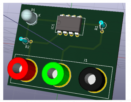
KiCad’s integrated 3D Viewer helps you to view your PCB designs in 3D. An interactive 3D view helps to instantly inspect your design easier than with a 2D display. A large library of 3D models is offered. Rotating and panning around features help to inspect details.
The 3D Viewer can be launched by selecting a 3D viewer from an active project. This displays your board. The ray tracing renderer when enabled gets more accurate 3d views.
Gerber Viewer: Generating the Gerber Files
After modifying the PCB layouts and checking the design for errors, you need to get the boards fabricated. KiCAD provides all necessary files for PCB manufacturing (Gerber files, drilling files, component location files).
To generate Gerber and drill files, open your PCB design file and go to File -> Plot. This will launch the plot window that will help you select the layers of the board and other features of the Gerber files that should be generated.
This file can be then sent to your favourite PCB manufacturer. KiCAD supports the capable Gerber file format Gerber X2.
Run a Simulation
Performing a simulation is a good thing for a quick inspection of your design before sending it for fabrication. KiCAD offers an open-source SPICE based simulator ngspice that allows you to perform analog, digital and mixed-signal simulations.
ngspice provides simulation capability in graphical form through integration with the Schematic Editor. You can launch the simulator directly from the schematic editor.
You can configure four standard simulation modes: AC Sweep, DC Transfer, Operating Point and Transient.
Furthermore, you can define your own custom simulation. You can run simulations and use the probe tool to select nets to plot voltage and pins to plot current.
PROs and CONs of KiCad
PROs:
- Open source: KiCad is open source making its source code available for anyone on the internet.
- Free: It is free to download. There are no trial or standard versions.
- Cross-platform: KiCAD is cross-platform. It works for Mac, Windows or Linux users.
- User interface: To enhance productivity, the user interface (UI) is designed well with easily accessible tools which can be re-arranged to personalize the workspace. Thus, it is easy to use by users with no prior schematic/PCB development experience.
- There are no restrictions on the number of layers or pins and size of the board, as well as who can manufacture your board.
- Professional-grade features: KiCad has great design features to help you work on complex designs such as differential pair routing, interactive routing, etc. Furthermore, being open-source, it gives a flexibility to users to add third-party features such as auto routers.
- Community: The KiCad community supports the KiCad project by sharing tutorials, codes, guides, libraries over the internet.
- A dedicated team of developers helps to constantly accelerate and improve the KiCAD project.
- Simulation: KiCad integrates a SPICE simulation engine. The schematic drawn in Eeschema can be simulated in SPICE.
- Many innovative utility tools: Bitmap2Component – this feature helps you to import and convert an image file in all major formats into a PCB footprint; PcbCalculator helps to calculate components for regulation, transmission lines, etc; Pl Editor is the Page layout editor.
Cons:
- KiCad lacks the team collaborative features.
Enhanced Design Capabilities
- Integrated 3D Viewer – Inspect your PCB layout in 3D for easy error detection and visualization.
- Modular and hierarchical design Support – Ideal for huge projects that need to be divided into manageable chunks.
The first release date of KiCAD was in 1992 and the latest release of the software, KiCad 5.1.12, was released in November 2021. If you want to download the latest version of this open-source KiCad EDA, click here.
For reading other similar reviews: click here
This article was first published on 27 December 2021.


