


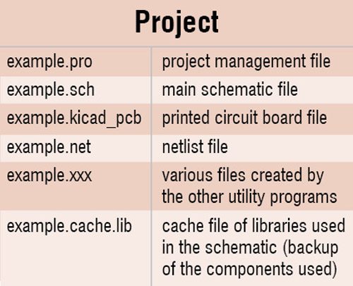
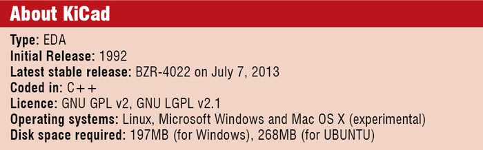
Operational on Apple OS X, Linux and Windows, KiCad is an electronic design automation software tool to design and generate professional schematics and printed circuit boards. A well-known software tool, KiCad is released under the open source General Public Licence v2 (GNU GPL).
Abhishek A. Mutha
Designed and written by Jean-Pierre Charras, and under active development by the KiCad Developers Team, KiCad features an integrated environment that allows you to create schematic diagrams and PCBs up to 16 layers.
KiCad can be implemented and interoperated on multiple computer platforms. It is an open source software suite for EDA and it facilitates the design of schematics for electronic circuits and their conversion to PCB designs as well. Basically, it provides the user with an integrated environment for PCB layout design and schematic capture.

 Tools exist within the package to create a bill of materials (BOM), artwork and Gerber files and 3D views of the PCB and its components too. A number of component libraries are available with the ability to add custom components by the users.
Interestingly, there are tools available to assist with importing components from other EDA tools like Eagle, for example. With multiple language support and 3D PCB viewing, there is a built-in basic autorouter as well.
Features and functionality in three steps
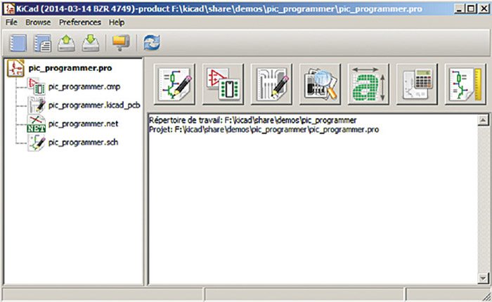
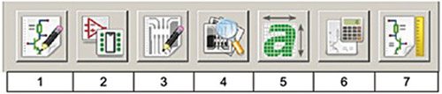
KiCad allows you to develop your printed circuit board (PCB) via three interconnected and independent main applications: Eeschema, Cvpcb, Pcbnew. This is simply done in three steps.

Step 1: Schematic capture. With the KiCad schematic editor Eeschema, you can create a sophisticated electronic sheet or a group of hierarchical sheets. Several schematic components come with the default KiCad library. An Electrical Rules Check (ERC) tool is available too.
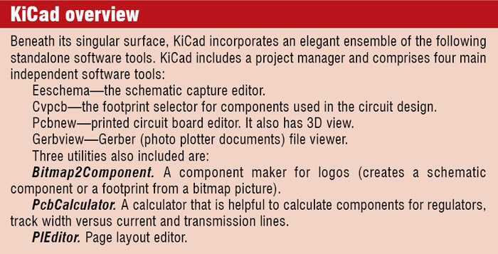
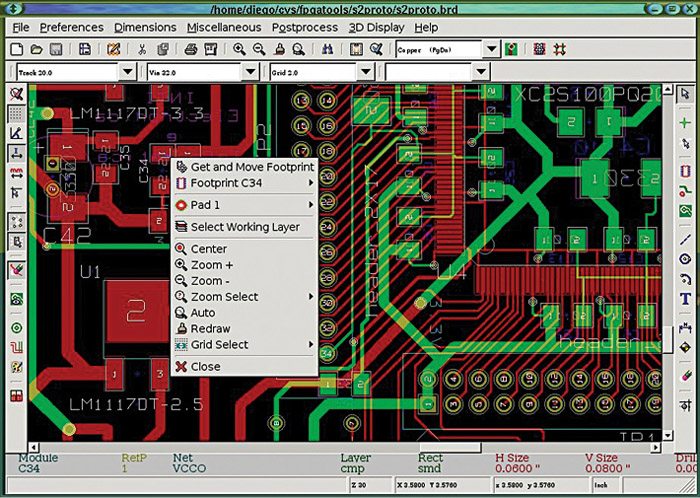
Step 2: Component association. Cvpcb allows you to associate each single schematic component with its footprint component. A very large component footprint library comes with KiCad.
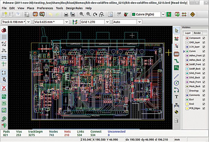
Step 3: PCB layout. The Pcbnew board editor can handle up to 16 copper layers plus 12 technical layers (silk screen and solder mask) and allows you to layout the final PCB.
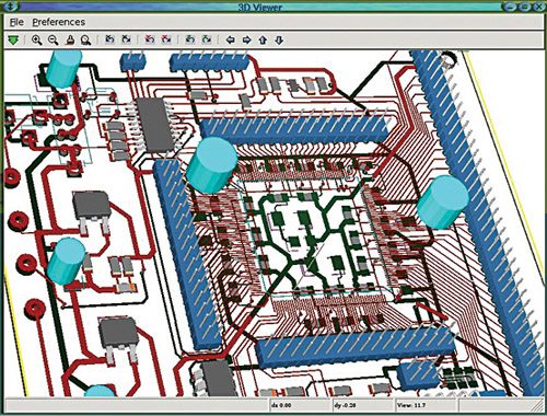
 To successfully perform these steps, KiCad comes with additional software tools. Two library component editors allow you to create or modify schematic components and footprint components. The 3D viewer allows you to render a final 3D model of your PCB.
For the generation of the necessary compliant files for manufacturing, your PCB (Gerber files for photo-plotters, drilling files and component location files), Pcbnew and Gerbview are used. Postscript or PDF file generation is also possible.
What one can do with KiCad
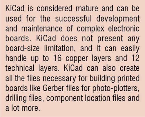
KiCad is considered mature and can be used for the successful development and maintenance of complex electronic boards. KiCad does not present any board-size limitation and it can easily handle up to 16 copper layers and 12 technical layers. KiCad can also create all the files necessary for building printed boards like Gerber files for photo-plotters, drilling files, component location files and a whole lot more.
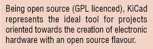 Being open source (GPL licenced), KiCad represents the ideal tool for projects oriented towards the creation of electronic hardware with an open-source flavour. It is an excellent tool for professionals and hobbyist, mainly due to the excessive cost of commercial software that are prohibitive for students and hobbyists.
With the help of the project manager, one can start the creation of a project by launching Eeschema. It manages a direct and fast access to component documentation. Eeschema is an integrated package because it comprises all the functionalities such as library management, layout, drawing and control to name a few. Using multi-sheet diagrams, it allows hierarchical drawings—simple, complex and flat hierarchies. Needed for modern schematic capture, Eeschema provides some essential additional functions such as:
1. Design rules check (DRC) for the automatic control of incorrect connections, and the inputs of components left unconnected.
2. Export of the layout files to POSTSCRIPT or HPGL format.
3. Printing the layout files on a local printer.
4. BOM generation.
5. Net list generation for PCB layout or simulation software.
KiCad component libraries
KiCad comes with a large set of open source library components. A text-based format is used for both schematic and PCB components. This allows the direct editing of your library files with any text-based software.
Both Eeschema and Pcbnew have a library manager as well as a library component editor for modifying and creating components and footprint parts. You can create, edit, delete or exchange library items easily. Documentation files can be associated to components and footprints, and key words, allowing a fast search by function. Very large libraries, created over many years, are available for schematic components and footprints. Most of printed board modules (footprint) are available with their 3D shape model.