


A free, easy-to-use computer-aided design software package for Windows platform, that lets you design printed circuit boards of professional quality very quickly
Anagha P.
Several electronic design automation (EDA) software are available in the market, which provide professional-grade printed circuit board (PCB) designs. While the premium and full-featured versions of design software can be pretty expensive, there are several alternatives in the form of free integrated design environments (IDEs) available these days.
ZenitPCB is one such excellent EDA toolset that allows PCB designing for electronics projects. This freeware is flexible, has a simple user interface (UI) and lets you realise the design in a short period of time.
This design suite comprises four tools: ZenitPCB Layout, ZenitCapture Schematic, ZenitPCB Parts and ZenitPCB GerberView.

Why ZenitPCB
the ZenitPCB software package is absolutely free of cost and still provides designs with professional levels of accuracy. It comes with some advanced features offered by paid software—extensive and well-managed library, multiple layers and double-sided designs support, high flexibility, superior schematic design, compatibility with standard design file formats and a tool for viewing Gerber file.
The software reduces the time to market; for example, the user can import a mechanical drawing with a PCB and build his/her board outline, thereby avoiding mistakes and saving time.
Who can use it
ZenitPCB Suite and the accompanying libraries are licenced as freeware and can be used for personal, educational and semi-professional purposes. It is aimed at designers, engineers, hobbyists, students and academicians who want to create their own PCBs with a professional touch, without having to pay for expensive licences. The circuit board for design has 800 pins and serves the level of complexity that would be required by designs for the targeted audience. This 800 pins limit, according to the developer, is the borderline between the hobby projects and professional jobs.
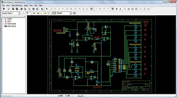
Designing schematics with ZenitCapture
 Schematic designs can be created quickly and easily using the feature-rich toolset of ZenitCapture.
A schematic in ZenitCapture can have several layers and the layout is created in a netlist file format. The part libraries have a collection of more than 800 commonly-used components (both surface-mount devices and through holes) suitable for immediate placement on the project. The device required for design can be either selected from these libraries or edited/created using ZenitParts.
Connections can be easily added with orthogonal locking and snap-to-pin features. You can also place global symbols (ground pin – GND and power supply pin – Vcc), IEEE symbols (Sigma – Σ, Pi – Π, bidirectional arrows – ↔, hysteresis – ⎎ etc), off-page connector symbols, wires, shapes, texts, field texts and so on in the schematic. Other features include auto-renaming of reference, ability to mirror the parts, customisable colour schemes and visibility for each of the layers, availability of datasheets on parts provided in the library, option to export netlist format files into PCB and customisable ASCII report.
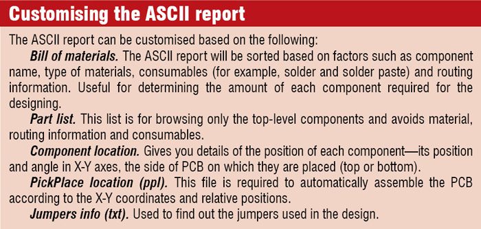
 ZenitPCB allows the export of reports into ASCII files into either no separation (as image) or separated (comma-separated values or CSV—to import into spreadsheet).
 ZenitPCB layout tool lets you use Netlists from competing software
This tool allows the user to import a netlist file from various other major schematic capture software (OrCAD by Cadence Design Systems, Protel/Altium Designer by Altium Limited, EAGLE by CadSoft Computer, NI Multisim by National Instruments Electronics Workbench Group, PADS by Mentor Graphics, to name a few) while preserving all the components and their relative electrical connections.
Design without schematic. It is also possible to create the PCB design project directly from the layout editor, without the need for importing netlist from schematic capture. This can be done by importing components from the library and then connecting those pins using the cursor (auto ratlines).
J umpers. Jumpers are short pieces of conductors that let you bypass part of a circuit and make electric connection between two pin headers. The current version has an autojumper introduced to it. When routing, you can import jumper decals into the project and place the selected surface-mount jumper on the top or bottom side of the PCB.
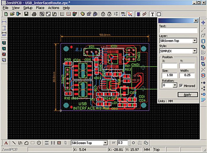
Photo View. This view gives you the idea of how the real PCB would look like; it shows all the through holes, slots and silk screens. The user can check whether the components are placed in the correct side, the silk and references are placed well or end up on the pads.
Rename Components. The AutoRename Reference command allows you to rename all the components in the layout. You could choose whether they should be numbered horizontally or vertically, and the width of the band. Also, you will be able to create ASCII for back annotations of several schematic captures.
