Electronic product design is never a single-step process. Right from conceptualisation of the idea to its fabrication and packaging, the design should account for a variety of factors. The traditional electronic design environments make use of a divide-and-conquer approach. Here, each step is implemented separately on different platforms. These are later integrated to form a single design. This might result in the omission of some minute but crucial details, besides reframing and eating-up your limited budget. Also, you might not be able to meet your project deadlines, which can risk the time to market.
Altium Designer from Altium is a one-stop electronic design environment that integrates schematic capture, PCB design, FPGA design, embedded-software development and manufacturing file support into a single unified application. Ultimately, this can help you eliminate data-translation and synchronisation issues.
What is new in Altium Designer 15
Altium Designer 15, the latest version of the software released in November 2014, comes with a powerful array of new features and enhancements to its core technologies. This version has also addressed some issues that were raised by the customers. Let us take a look at some of them.

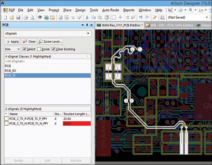
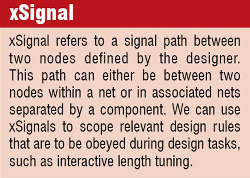 xSignals for high-speed designs. The signal-propagation rate in modern designs is very high and can even rise to 100 gigabytes per second. Deciding the design rules is not easy at these propagation rates. The reason is simple. While the designer sees the function of the signal, PCB editor can only view the signal as a set of connected pins. This makes it difficult for the design engineer to specify key requirements of his design, such as length and matched-length design rules.
The new feature from Altium called xSignals is introduced primarily to resolve this issue. xSignals helps the designer to treat the high-speed signal path in exactly the way he wants. That is, as a path in which the signal travels between the source and destination covering the termination components and branches. This path helps the designer to accurately plan and route groups of high-speed nets with more efficiency.
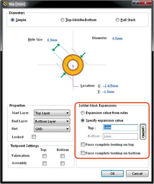
Solder mask-expansion enhancements. In today’s PCB designs, there are situations where we need different expansion settings for top and bottom layers of applied solder masks. Altium Designer 15 is now equipped with pad and via-expansion settings by which we can have individual configurations for top and bottom layers.
PCB rules and constraints editor can be used for defining and modifying solder mask-expansion rules for the board pad and vias.
Separate 2D and 3D view orientations. In previous versions of Altium Designer, on switching from 2D view to 3D, or from 3D to 2D, the region of focus remains the same. But these two views are completely separated in the latest version. Each view retains the orientation, zoom and layer configurations of its previous display.
We can also have an in-depth examination of design-type features by clicking cntrl+cntrl.
IDX MCAD integration support. Electronic designs, nowadays, involve more and more electrical and mechanical components. This calls for an increased collaboration between the electrical and mechanical computer-aided design (ECAD and MCAD) domains. Unfortunately, engineers working on these domains use different design tools, and communication between them is not so easy.
As a solution, a collaborative standard known as incremental design exchange (IDX) format has been introduced. This standard enables the two to graphically communicate ideas and proposals for change, without leaving their trusty working environments. Support for this standard of collaboration between ECAD and MCAD domains is available in Altium Designer 15. It will help in easy synchronisation of the enclosure model, board shape and component placement for the best mechanical fit.
What to expect
Reviews from various forums suggest that users are very satisfied with this product. A blogger feels that Altium Designer is a good product for a good price. Initially, he was suspicious about the online services given by the company. He mentioned that, if the user becomes dependent, the company could charge him more. But Altium is altogether different, concludes the blogger from his experience.
Another user feels, “The graphical interface of this tool is the first thing that I noticed. The software looks new and fresh as compared to other CAD tools. The library consists of one single file. All CAD tools should follow this model. It makes transferring and sharing your library a breeze. Copying components from one library to the next is a simple copy-and-paste function. In general, the library manager could not be much better. The wizard has many component types to choose from and is very easy to use. All objects can be modified using the property option, which gives the designer lots of flexibility. The measure function is very good as well and provides all necessary information (centre to centre, edge to edge).”