


Most free or low-cost PCB editors are either limited by pin and layer limits, or have bugs that make them difficult to use. So we have found a better one for you. Read this article to know more about the PCB editor called FreePCB
Pankaj V.
FreePCB, as the name suggests, is a free open source Windows program for editing and laying out PCBs. It is a handy tool capable of doing professional quality work, while at the same time remaining very easy to learn and use for beginners.
FreePCB comes with an intuitive GUI and options that allow you to perform almost any task related to PCB designing. It can easily be used for serious designs too, as it can handle multiple (up to 16) copper layers and comprises a Footprint Wizard and Footprint Editor for guiding the process of creating or modifying your footprints.

 You can configure the footprints using the various functions that come bundled with the software. I also found an interface to the FreeRoute autorouter program, which relieves you from manually routing each trace in your design, thus making the design process much easier. Let us take a deeper look at the key features.
Key features
The other PCB tools, including some paid ones, can be far too intimidating and overly complex, but FreePCB is quite easy to use and learn. There are enough features in this tool for your PCB design requirements. Let us look at each of the important benefits and how they stack up.
User-friendly tool. Apart from the obvious PCB design functionality, some built-in features also exist which make working with FreePCB user-friendly. To list a few, we can start with the ‘auto-save’ feature. the auto-saved files are stored in a subfolder of the project folder, with incremental file names generating automatically.

File handling gives the advantage of re-usability, groups can be saved as project files and you can paste a project file as a group into another project. Automatic functions such as Check Traces clean up traces for you by combining collinear segments and eliminating zero-length segments. Also, you can make changes in the settings for a pin and applying those to other pins in the Footprint Wizard.
We cannot list all but, using this tool, you will find many other useful features which will make your PCB designing process very easy and efficient.
Footprint wizard and footprint editor. The software comes with a wizard kind of tool that helps you in creating footprints easily, so that you do not have to labour through the process like in some other tools.
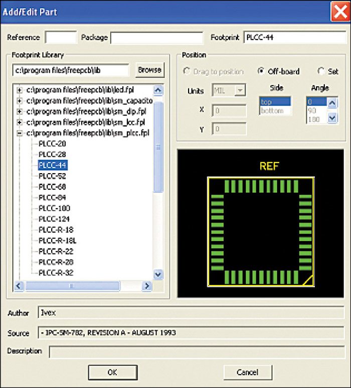
Apart from the footprints available in the Footprint Library, you can create footprints for a variety of standard packages using this wizard and edit those existing ones using Footprint Editor. You can also add and edit the pins in the footprints, eliminating any limitations that are usually seen with competing products.
Import netlist from any schematic editor. If you already have a favourite schematic editor, you do not have to leave it while moving over to FreePCB. While you can surely generate a netlist within FreePCB, you also have the flexibility to import it from any other schematic editing program that can output a PADS format netlist. Moreover, once you do this, you can then manually place the components and route traces between the pins of the components to continue work.
Design rule checking. Practically there are certain lower limits on trace widths, pad sizes and clearances between copper features and/or holes, called Design Rules which vary depending upon the manufacturing process that you plan to use, should your design be approved for production. FreePCB has a Design Rule Checker which checks your PCB design for compliance with a set of design rules provided by the PCB manufacturer.
Easily share output. The person to whom you send your file does not need to have a copy of FreePCB to be able to view it, as there are multiple ways in which the file can be shared with others for viewing. The tool outputs RS-274X-formatted Gerber file data and a drill file, which you can use to make boards of sizes up to 152cm by 152cm. There also are many options available for Gerber file outputs and dimensions, as per your requirement, which can be viewed in any free Gerber Viewer.
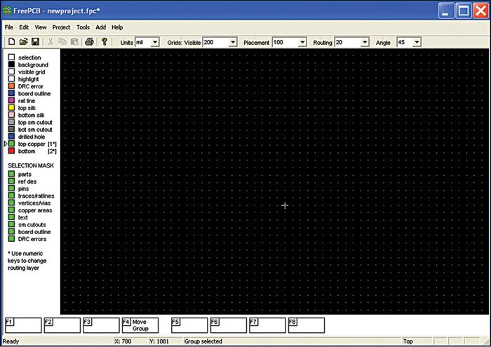
Decent GUI. The main elements of the GUI window are the menu bar, the taskbar immediately below the menu bar and the layer list on the left side of the client area, showing its colour and visibility, the selection mask below the layer list, with options to enable/disable selection of various items, the layout window showing the PCB, the function key menu below the layer list and layout window which shows the available function key commands and the status bar at the bottom.
