Wide adoption of standardised IEEE 1149.x test methods has called for the independent and non-commercial platform-based tools for JTAG test principles. goJTAG is a JTAG/boundary scan tool which offers a clear illustration of the standard test principles. Read this article to get an insight of how to start working with it
Pankaj V.
The well-established test technique boundary scan JTAG IEEE Std. 1149.x is a unique solution to many test requirements and provides information about the board without accessing the complete board. Therefore it is ideal for testing the complex boards which could not be tested otherwise due to lack of test access. Boundary scan systems have little hardware and their significant part is software.
 goJTAG is a part of an open source project which provides a full package for a JTAG newcomer including training material, slides and exercises. The software allows you to study boundary scan techniques, carry out your own experiments, perform diagnosis and much more. The software environment comes with a built-in example project, and you can create your own projects with descriptions of boards, chips, cluster logic and so on.
goJTAG includes a simulation component fully illustrating the underlying concepts of JTAG/boundary scan that allows you to directly step-wise control the test features of IEEE 1149.1-compliant devices and observe a system’s reaction in real time in an on-screen simulation environment.

Starting with goJTAG
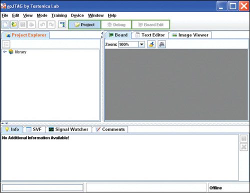
After successful installation of the software, you can run it, which will open a GUI environment providing you with various options to control the test features of IEEE 1149.1-compliant devices.
Working modes. There are three working modes supported by goJTAG:
1. Project Mode allows you to view/organise your project items, create or import new files
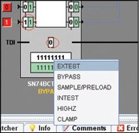
2. Using Debug Mode, you can perform boundary scan operations such as select instructions, perform scan, define test vectors, observe diagnostic results, amongst others.
3. In Board Edit Mode, you can create/edit your own netlists.
For changing the mode, just select the appropriate mode from the dropdown Mode menu. Alternatively, you can select the corresponding special toolbar buttons at the top.
Note: You should start your work with Project Mode to choose the netlist first.
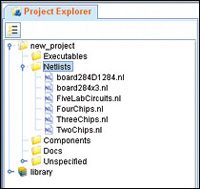
Opening netlist. After creating a new project from File→New→Project, you should first choose a netlist to work with. Expand the project tree from Project Explorer space to netlists group and choose one of the available netlists; Netlists are stored in files with .nl extension. To open any netlist file, just double click on it and you can see the boundary scan devices in the corresponding netlist in the Board panel.
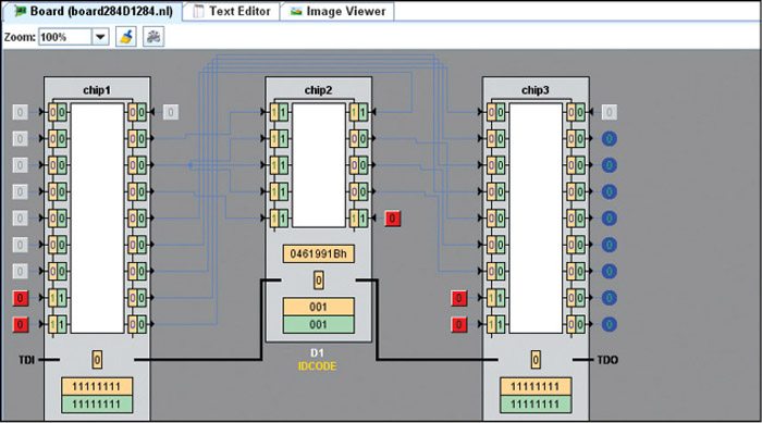
Board. After opening a netlist, the boundary scan circuitry of board can be visualised on the Board panel. Now you can see boundary scan devices, boundary scan cells, instruction and bypass registers, IDCODE/USERCODE registers (if present), connections between chips, external input/output (I/O), etc. If the description of the internal logic is present in the board description, full simulation becomes available. The colours of signal lines represent the current signal values. The Info panel at the bottom shows the information about the corresponding netlist.
Boundary scan operations. To start performing boundary scan related operations, you need to switch to the Debug mode, which will open a Test Constructor panel in the left.
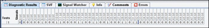
In this panel, you can specify instruction and test patterns for each boundary scan device. After specifying the instruction and the test patterns, press the Run button to start performing scan. Additionally, you can also perform scan IR and scan DR operations separately by pressing the corresponding buttons. The results of scans are displayed in the Diagnostic Results panel at the bottom.
Note: You can select the instructions and input scan values directly on the board by simple right clicks and selecting the desired register.
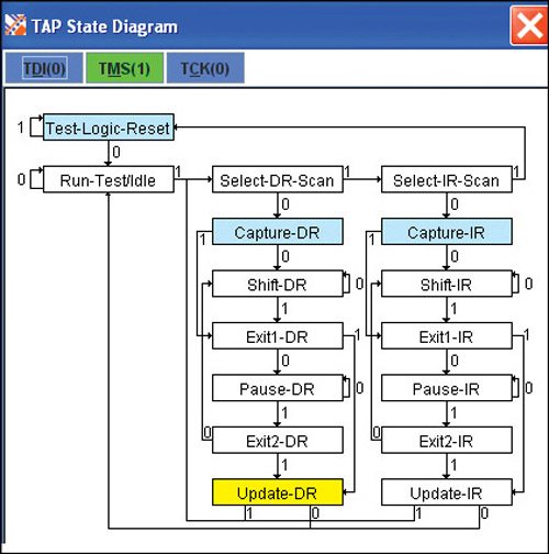
TAP controller. The software also allows you to control the TAP controller of a boundary scan device directly by visualising its state machine. Select Window→Tap State Diagram menu or press the Tap State Diagram button at the toolbar to display the TAP State Diagram.
You can click TDI and TMS buttons to change input signals. Pressing the TCK button, a clock cycle is generated and the TAP controller might change its state depending on the value of TMS. If you hold Shift key and then press the TCK, it will generate clock edges.
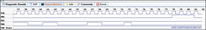
Also, you can speed up your work with TAP controller by clicking on the highlighted states. In this case, the software will generate the required sequence of TCK/TMS signals automatically. Signal Watcher panel at the bottom shows how signals and TAP states change.