Electronics design engineers require a number of software to create and verify their designs digitally, before moving to production. KiCad brings all these tools together under one platform, making their tasks simpler. This free electronic design automation (EDA) software suite mainly comprises a schematic creation and capture suite, and a PCB layout tool. It enables operations like creating bills of materials (BOMs), gerber files and PCB 3D views. Running under GPL v3 licence, this open source suite runs on Windows, Linux and MacOS.
Components of KiCad
KiCad suite integrates a number of popular open source tools for various EDA functions. The process incorporates the following steps: schematic creation, netlist generation, layout building and simulation. Given below are the tools that majorly make KiCad suite.
Eeschema
It is an interactive schematic creation platform that comes in KiCad suite. Eeschema brings a graphics-based design area that can create schematics with simple click operations. KiCad library is extensive and brings symbols, footprints and 3D models of almost all major components that are required for the circuit. This allows you to build any scale of circuit schematic on Eeschema.
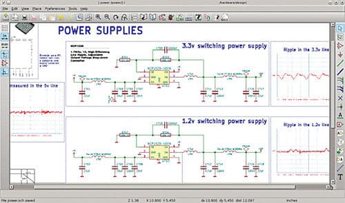
Complex schematics can be broken into sub-circuits or into hierarchical circuitries. Many quick access buttons for components enable swift schematic creation.
Eeschema also supports imported components library. This can be accessed from Preference menu.

Eeschema helps you verify your circuits through electrical rules check (ERC). It can point any conflicts in the output pin, unconnected pins or missing drivers. The schematic can be captured in a variety of formats, including netlists, which can be exported in various formats like Pspice, Cadstar, PcbNew and Generic XML. BOMs can also be generated using Eeschema. Buttons for both BOM and netlist creation are available on Eeschema’s toolbar.
PcbNew
This tool is used to design the layout based on the schematic and netlist generated. PcbNew suite has recently been upgraded with a new graphics abstraction layer (GAL) engine, Cairo and OpenGL libraries. For circuit routers on PcbNew, KiCad employs a built-in routing tool as well as Toporouter. A new push-and-shove router feature ensures compliance to design rules check (DRC).
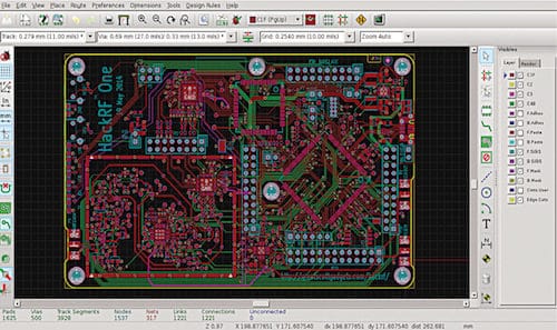
PcbNew workspace brings a host of options and features. It supports layer-based operations, making multi-tiered or complex circuits easier to lay out. You can optimise trace lengths for high-speed designs with the help of its length tuning feature.
Interface of PcbNew is smooth and compact. More functionalities can be accessed across the interface. More latest upgrades of PcbNew include differential pair support and Python scripting support. A 3D view of the PCB layout can be also exported.
More tools
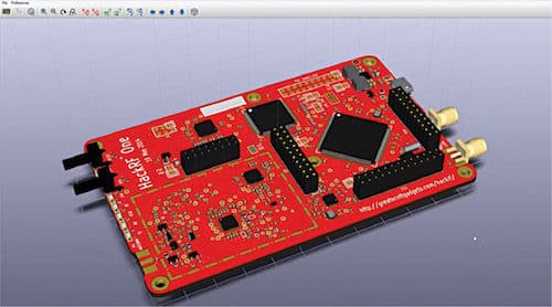
KiCad brings another tool so that you do not have to look outside for 3D viewing of a PCB model. It can be done using 3D Viewer tool. You case access 3D Viewer from View menu of PcbNew suite. The circuit board can be rotated in all directions by simply dragging the 3D image with the help of the mouse. You can zoom in or out, change colours while viewing and do more operations with this tool.
KiCad’s main Gerber file viewer tool is GerbView. GerbView supports RS-274D and RS-274X Gerber formats. Older files can be converted into this format as well. The workspace supports multiple files simultaneously. GerbView provides elements like markup tools (text, barcodes, QR-codes, images, etc), measuring tools (for distances, areas, etc) and so on. A circuit can be exported, as a single layer or the whole design, in various formats like TIFF, JPEG, PNG, BMP, PDF, DXF and DWF.
Another tool, Bitmap2Component, converts image files to design layout footprints.
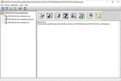
Finally, there is KiCad project management suite that lets you access projects and get various information about them.
Getting started
After installing KiCad, the first window on startup shows the various programs of KiCad that can be opened, in addition to main menus like File, Browse, Preference, Tools and Help.
From File menu, you can open an existing project or create a new one. A project contains four major file types: .pro, which is the project file; .cmp, which is the components file; .kicad_pcb, which is for PCB layout and .sch, which indicates a schematic file.
You can open each file in the respective tools. Alternatively, you can start a new project from scratch. The first tool opened will be Eeschema. Once you create the schematic and save the netlist, you can use it in PcbNew.
KiCad comes with enough documentation and tutorials to guide you at every step. An active community support comes useful to solve any configurational error(s). Overall, KiCad is a complete EDA suite with easy-to-use tools. It can be used by students, hobbyists and professionals alike.