

For the language and font settings to take effect, the application (as seen in Fig. 2) must be closed either via the Ctrl + Q shortcut or the File → Exit menu entry. Then re-start Qucs.
Setting up schematics
The following sections will enable the user to set up some simple schematics. For this, first create a new project named ‘WorkBook.’ Either press the New button above the projects folder or use the menu entry Project → New Project, and enter the new project name as shown in Fig. 3.

Confirm the dialogue by pressing the Create button. When done, the project is opened and Qucs switches to the Content tab.
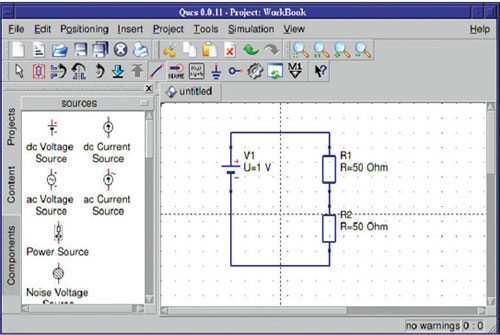
In the Content tab, as seen in Fig. 4, you will find all the data related to the project. It contains your schematics, the VHDL files, data display pages, datasets as well as any other data (like datasheets). On the right hand side, an untitled and empty schematic window is displayed. Now you can start to edit the schematic. The available components can be found in the Components tab.
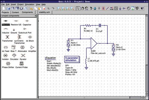
The window in Fig. 5 is displayed on clicking the Components tab. There are lumped components (such as resistors and capacitors), sources (such as DC and AC sources), transmission lines (like microstrip, coaxial cable, twisted pair), nonlinear components (like ideal op-amp, transistors), digital components (like flip-flops), file components (like Touchstone files, Spice files), simulations (AC or DC analysis), diagrams (like Cartesian or polar plot) and paintings (such as texts, arrows, circles).

Each of the components can be placed on the schematic by clicking it once. Then move the cursor onto the schematic and click again to put it on its final position. You can right click to rotate the component into its final position. You can even drag-and-drop the components.
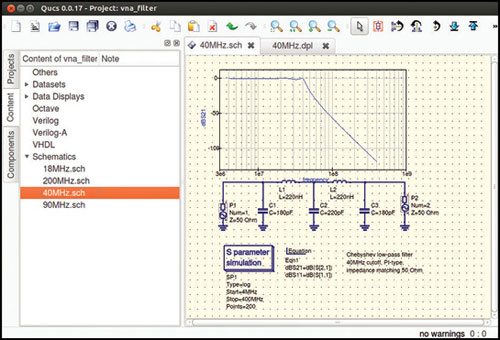
DC simulation of a voltage divider
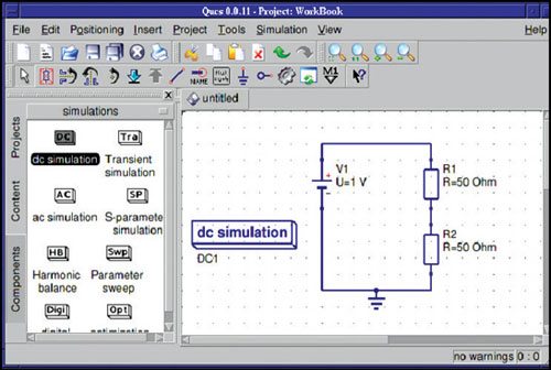
DC analysis is a steady-state analysis. It computes the node voltage as well as branch currents of the complete circuit. The circuit in Fig. 6 is for dividing the voltage of a DC voltage source according to the resistor ratio.
Wiring components. Connect the components appropriately using the wiring tool. Enable the wiring mode either by clicking the wire icon or by pressing the Ctrl + E shortcut. Left clicking on the components’ ports (small red circles) starts a wire and clicking on a second port finishes the wire. In order to change the orientation of the wire, right click it. You can leave the wiring mode by pressing Esc key.

For any analogue simulation (including the DC simulation), there is a reference potential required (for the nodal analysis). The ground symbol can be found in the Components tab in the lumped components category. The user can also choose the ground symbol icon or simply press the Ctrl + G shortcut. In the circuit in Fig. 7, the ground symbol is placed at the negative terminal of the DC voltage source.
Placing simulation blocks. The type of simulation that is to be performed must also be placed on the schematic. You can do this by choosing the ‘DC simulation’ block, which is found in the Components tab in the simulations category.
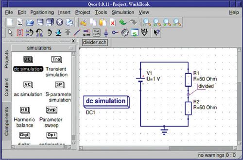
Labelling wires. If you want voltage between the two resistors (the divided voltage) be output in the dataset after simulation, you need to label the wire. This is done by double clicking the wire and giving it an appropriate name. Wire labelling can also be done using the icon in the toolbar, by pressing the Ctrl + L shortcut or by choosing the Insert → Wire Label menu entry.
The dialogue is closed by pressing the Enter key or pressing the Ok button. Now the complete schematic for the voltage divider is ready and can be saved. This can by done by choosing the File → Save menu entry, clicking the Single Disk icon or by pressing the Ctrl + S shortcut.
The final DC voltage divider is shown in Fig. 8.
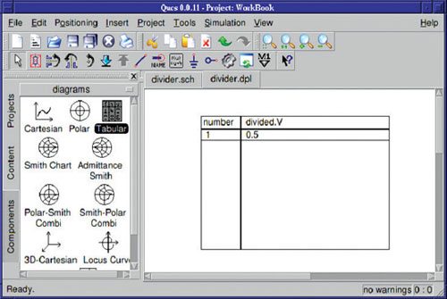
Issuing a simulation. The schematic can now be simulated. This is started by choosing the Simulation → Simulate menu entry, clicking the simulation button (the gearwheel) or by pressing the F2 shortcut. After the simulation has been done, the related data display is shown. Also, the Components tab changes its category to ‘diagrams.’
Placing diagrams. Choose the tabular (list of values) diagram and place it on the data display page. By double clicking ‘divided.V’, the graph (values in a tabular plot) is added to the diagram. Besides the node voltage ‘divided.V’ the current through the DC voltage source V1.I is available. Only items listed in the dataset list can be put into the graph.