
For professional electronic circuit designers and even DIYers who want to test their design before physically animating it, ZenitPCB can be a great tool. This Windows-compatible PCB design suite allows designs with up to 1000 pins.
The complete ZenitPCB suite consists of multiple tools. ZenitPCB Layout tool lets you design the main layout of the printed circuit board by using a netlist of components to be used. ZenitCapture Schematic tool allows you to choose components of the circuit and create a netlist. ZenitPCB tools are contained in a library called ZenitPCB Parts. The software can also read Gerber files through its PCB GerberView tool.
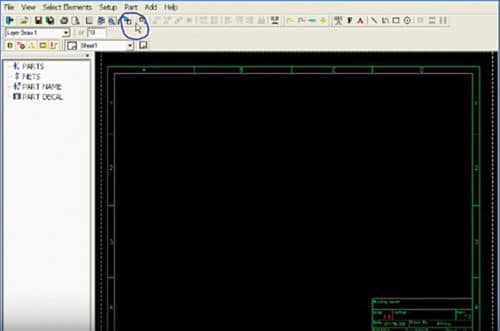
The user interface of ZenitPCB is compact—even with numerous application buttons and quick keys. It contains the main workspace in the middle. Below the menu bar, on the top, there are multiple quick-access keys that allow you to add circuit parts, save a file, print, search and so on. The left panel consists of project-related information including available projects, parts library and available netlists. To the right of the workspace there are shortcuts for different operations like drawing a line, square or circle in the schematic, adding text and so on. The workspace allows simple drag-and-drop operation, so handling the tool is simple.
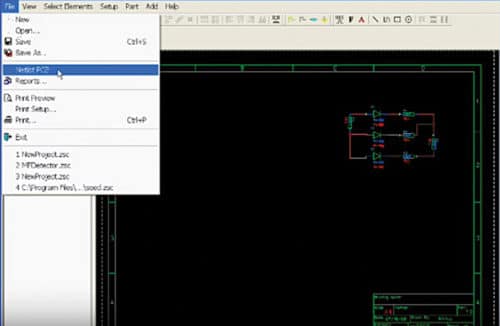
To start a new project, go to File on the top menu bar and click New. This will open a workspace on the ZenitCapture Schematic tool. The workspace is a sheet in black with green borders giving the position of elements to be placed. Now, you can select components and create your circuit schematic. Components can also be selected from the quick-access button below the top menu bar.
First, click the desired element and then click on the workspace to position it. As soon as you add your first component, you will see a ‘+’ sign appearing beside Parts option in the left panel. This indicates component addition to your circuit and netlist creation. You can expand this option to check out all the elements added. Elements can be connected by simply dragging (through the mouse) the connection point of one component and linking it to another. When you have prepared your schematic, you need to pack it in a netlist. Go to the top menu bar of the ZenitCapture Schematic. You will find multiple menus including File, View, Select Elements, Setup, Part, Add and Help. Go to Part and click Package Parts. Now, go to File and click Netlist PCB. Save the file. Your netlist is now ready for use in the layout.

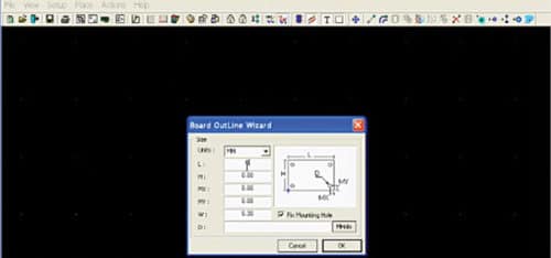
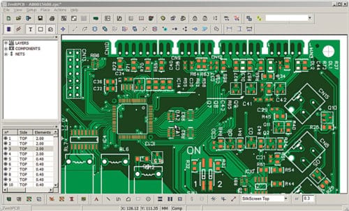
Next, go to ZenitPCB Layout tool and open a new project. Choose your PCB size and dimensions. This can be done by clicking Place in the top menu of this tool and then choosing Board Wizard. Next, set up your components in the layout board. Go to File and select Netlist under Import. Choose the netlist you want to use. Once the components are imported, place them on the digital board. You can modify components by right-clicking these in the workspace.
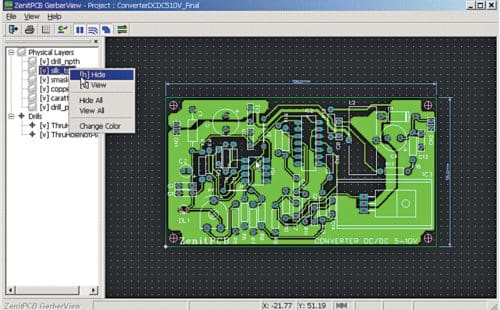
To view Gerber files, click ZenitPCB GerberView button and choose the file. The program can open Gerber and NCDrill files and provide visualisation according to ASCII format.
Users can change layer colours in the visualisation or even hide layers for better viewing. The left panel shows physical layers and Drills available in the Gerber file.
What’s new
The latest version of ZenitPCB includes many improvements with issues fixed in all tools. In addition, new functionalities have been introduced. One of the most significant upgrades is the addition of 200 more pins, which allows users to use up to 1000 pins instead of 800 in the previous version. In ZenitCapture Schematic tool, features like auto-change of parts values, placed parts listing, auto-renaming of Net wires and locking of open projects, alternative text printing and printing in black have been introduced. In addition, the software suite supports up to 1300 symbols. New features in ZenitPCB GerberView tool include hiding of layers during view, mirror view, printing (in centre page, printing in black and printing holes) and print preview.
ZenitPCB is a very handy tool for practical circuit design. Explore all the options to check out the many possibilities that this software can deliver.
Download the latest version of the software