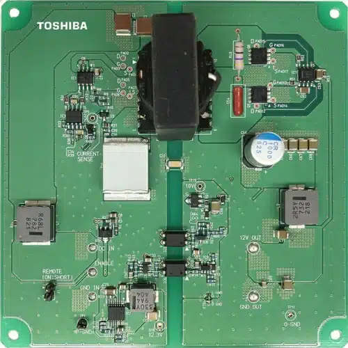
The converter design provides efficiency and compact design, suitable for industrial equipment and various applications, achieving 88% efficiency at full load.

The LLC DC-DC Converter is a highly efficient and versatile power conversion solution widely used in applications that require compact size, minimal heat generation, and stable performance. It operates with high efficiency by utilizing an LLC resonant circuit, which enables Zero Voltage Switching (ZVS) and significantly reduces switching losses, especially at high frequencies. This efficiency is crucial in applications like data centers, industrial equipment, and automotive systems, where energy savings, power density, and thermal management are priorities. By providing stable output with minimal noise and electromagnetic interference (EMI), LLC DC-DC converters play a vital role in modern power electronics, supporting advancements in performance and sustainability. A 100 W LLC DC-DC Converter reference design from Toshiba is suitable for use in industrial equipment connected to 24 V output AC-DC converters, as well as in various other applications.
The power supply generates a 12 V output using an LLC resonant circuit. The LLC circuit alternates the high-side and low-side MOSFETs on the primary (input) side at a 50% duty cycle, adjusting the switching frequency according to the load to regulate the output voltage. A dead time is introduced during the switching of MOSFETs to prevent the shoot-through phenomenon. During this period, ZVS occurs due to resonance, minimizing switching losses and contributing to high efficiency.
This power supply offers a total efficiency of 88% at full load and features a compact outline size of 110 mm x 110 mm x 35 mm, excluding input and output terminals on the backside. It utilizes optimized power MOSFETs and a photocoupler to enhance performance and reliability. In this power supply, the input voltage is stepped down to 12V by the LM46000 converter, which then supplies this 12V to the LLC controller to start the power supply’s operation. The input voltage range is determined by the resistance values of external resistors, which set the minimum operating voltage limits.
These limits are established by dividing the input voltage through resistors and feeding the divided voltage to the enable pin of the DC-DC converter. The converter begins switching when the enable pin voltage exceeds the threshold of 2.0V.
The design of the gate drive circuit significantly influences both power supply efficiency and EMI. Typically, there is a trade-off between achieving high efficiency and minimizing EMI, so a balanced design is essential. While the LLC circuit benefits from low EMI due to Zero Voltage Switching (ZVS) operation, switching noise can still contribute to EMI issues. The output voltage of the power supply is set by external resistors and a shunt regulator. The shunt regulator adjusts the current through the photocoupler to ensure that the voltage obtained by dividing output voltage with external resistors matches the reference voltage.
Toshiba has tested this reference design. It comes with a bill of materials (BOM), schematics, assembly drawing, printed circuit board (PCB) layout, and more. The company’s website has additional data about the reference design. To read more about this reference design, click here.


