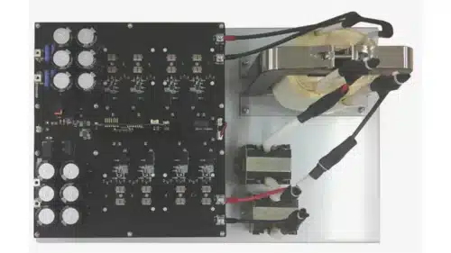
A 5 kW bi-directional DC-DC converter offers high efficiency and power handling, suitable for EV charging and photovoltaic inverters using the DAB method.

Toshiba’s 5 kW Isolated Bidirectional DC-DC Converter reference design is capable of delivering up to 5 kW of power. It can transfer voltage from the high-voltage side to the low-voltage side or vice versa. Utilizing the Dual Active Bridge (DAB) method, it emphasizes efficiency through a full-bridge configuration on both sides, allowing it to handle higher power compared to the half-bridge method. The DAB method enables soft switching via phase shifting, resulting in a highly efficient DC-DC converter suitable for various industrial applications, such as electric vehicle (EV) charging systems and photovoltaic power generation inverters.
The high-voltage input/output is designed for 750 V, requiring components that can withstand switching voltages of 1000 V or higher. Typically, an IGBT would be selected, but due to its significant switching losses, improvements in efficiency are limited. Instead, the design employs the TW070J120B, a 1200 V SiC MOSFET, to achieve both high-power and high-efficiency conversions. On the low-voltage side, with a 400 V input/output, the TK49N65W5—a 650 V MOSFET with reduced switching losses due to its super junction structure and integrated high-speed diode—is used to ensure high efficiency.
The gate driver features a 4 A sink-source current capability, adequately driving the gate charging/discharging current when switching the 1200 V SiC MOSFET. It uses the smart gate driver coupler TLP5214A, which includes overcurrent protection and a UVLO function. For the voltage-sensor circuitry requiring isolation, an optically coupled isolation amplifier, TLP7920, with high linearity accuracy and high common-mode transient immunity, is employed.
Some of the key features of the reference design include:
- High Voltage Side: DC 732V to 768V
- Low Voltage Side: DC 396V to 404V
- Rated Power: 5.0kW
- Circuit topology: Dual Active Bridge(DAB)Conversion Method
The design of the gate drive circuit significantly impacts power supply efficiency and EMI noise. Generally, there is a trade-off between power supply efficiency and EMI noise, requiring a balanced design approach. The power supply’s gate-drive circuit allows for adjustable MOSFET switching speed. To reduce noise at MOSFET turn-on, increasing the gate series resistor may help reduce EMI noise. However, this change will also reduce both turn-on and turn-off speeds of the MOSFET, potentially lowering power supply efficiency. To mitigate efficiency degradation, only the MOSFET turn-off speed should be increased by decreasing the gate series resistor.. This adjustment may enhance turn-off speed and improve system efficiency. When altering the gate series resistance, it is essential to ensure that the system’s EMI noise, power efficiency, and heat dissipation performance requirements are met.
Toshiba has tested this reference design. It comes with a bill of materials (BOM), schematics, assembly drawing, printed circuit board (PCB) layout, etc. You can find additional data about the reference design on the company’s website. To read more about this reference design, click here.


