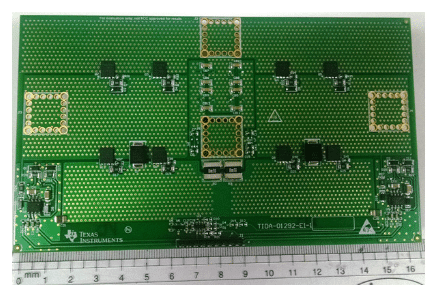
This reference design focuses on a 650-W inverter power stage suitable for low-frequency, transformer-based, single-phase Uninterruptible Power Supplies (UPS) that operate off a 12-V battery.

A power inverter is an essential device that converts electrical power from direct current (DC) to alternating current (AC) through sophisticated electronic circuits. Its primary function is to transform battery voltage into a standard household AC voltage, enabling the operation of household electronics in environments where AC power is otherwise unavailable.
The design TIDA-01292 by Texas Instruments leverages the technological advantages of the TI SMD MOSFET in a SON5x6 package, which is notable for its extremely low RDS(on) and minimal gate charge (Qg). This specific choice facilitates a compact and highly efficient inverter structure by utilising two parallel devices for each leg of the full-bridge power stage. This eliminates the need for a heat sink and reduces the overall system cost.
This design utilises eight CSD17573Q5B MOSFETs with a low RDS(on) of 0.84mΩ and reduced gate charge, enhancing efficiency by reducing power conversion and switching losses. Their 8-pin SON 5-mm×6-mm package aids in achieving a more compact design. Additionally, two LM5101B high-voltage gate driver devices control these MOSFETs, capable of handling both high- and low-side N-channel MOSFETs in configurations like synchronous buck or half-bridge. The floating high-side driver supports supply voltages up to 100 V and provides 2 A of gate drive capacity, with independently controllable outputs via CMOS input thresholds.
The INA181 handles the system’s current sensing and overcurrent protection. It is a bidirectional current sense amplifier that detects voltage drops across sense resistors at common-mode voltages from -0.2 to 26V, regardless of the supply voltage. It uses the A2 variant with a fixed gain of 50, integrating a matched resistor gain network to minimise gain error and temperature drift. The INA185 amplifier is available for applications requiring superior performance.
This inverter design is tailored for standby or offline UPS systems from 100 VA to 850 VA, expandable to 1.5 kVA with additional parallel FETs. Utilizing SMD MOSFETs improves manufacturability and simplifies assembly while eliminating heat sinks, which reduces costs and production time. Validated for 100-W to 650-W loads, the design typically achieves 95% efficiency, with peaks over 98.5%. It incorporates multiple protections, including overcurrent, short circuit, overvoltage, and undervoltage, making it versatile for applications like UPS, DC-to-AC inverters, energy storage, and residential inverters.
TI has tested this reference design with a Bill of Material (BOM), schematics, and other data. The company’s website has additional data about the reference design. To read more about this reference design, click here.


