 The accidental pressing of the on/off switch due to human error may cause the failure of the system it is connected to, or cause unnecessary delay to a part of the parent circuit. This could, in turn, cost money and time to reset/reboot the system.
The circuit presented here requires you to keep the on/off switch pressed for a certain duration to make sure that the action is actually intended and not accidental.
Circuit Explanation:
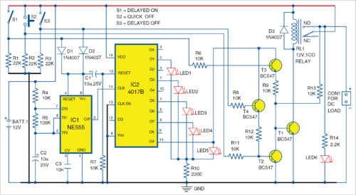
The circuit diagram of the accidental switching on/off protection using delay is shown in Fig. 1. It is built around NE555 timer (IC1), decade counter CD4017B (IC2), six LEDs (LED1 through LED6), four npn transistors BC547 (T1 through T4), 12V relay and a few other components.

The circuit employs 555 timer IC, wired in astable multivibrator mode, which serves as the clock source. Decade counter IC CD4017 provides visual feedback on how long you should keep pressing the on/off switch to achieve the desired action. Here, a 12V DC load can be connected to relay output, which is controlled through switches S1 through S3.
NE555 timer provides clock pulses to decade counter 4017B, which extends the delay provided by NE555. Delay timing of IC1 is decided by timing components, namely, resistors R4 and R5, and capacitor C2. LED1 through LED5 provide visual delay indication.
Except the relay coil in its energised state, most of the circuit consumes almost zero power when control switches are not pressed.
Working:
Working of the circuit is simple. On closing delay-on switch S1, transistor T3 conducts. Also, IC1 starts oscillating, IC2 starts counting and LED1 through LED5 glow one after another. And when IC2 counts to Q9 (at pin 11), its output turns on T1, relay RL1 energises. DC load connected across CON1 will be on after a prefix delay. Now, disconnect S1.
On pressing quick-off switch S2 momentarily, T2 and T1 conduct to switch off the load, as RL1 is de-energised.
On closing delay-off switch S3, T4 conducts. Also, IC1 starts oscillating, IC2 starts counting and LED1 through LED5 glow one after another. When IC2 counts at Q9 (at pin 11), its output turns on T2, RL1 de-energises to disconnect DC load after a prefixed delay. Now, disconnect S3. Refer table for details of switches and their functions.
Construction and testing
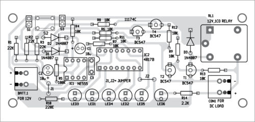
A PCB layout for the accidental switching protection circuit is shown in Fig. 2 and its components layout in Fig. 3. After assembling the circuit on a PCB, connect 12V battery across BATT.1 and 12V DC load across CON1.


Download PCB and component layout PDFs: click here
EFY note
To replace DC with AC load, you need another SPDT relay with its coil connected to existing relay output, or a single DPST/DPDT switch for replacing the existing relay (not shown in the circuit diagram).
Allen Mathew, Jestin T.A. and Jacob Abraham are electronics hobbyists


Can I get the proteus file of the layout??