


 Most square-wave generators have a single output that doesn’t have a high driving capability/slew rate or is not adjustable in the required amplitude range. Also, when conducting experiments or testing the electronic equipment, the errors are frequent and there is a high probability of damage to the digital generator output.
So it is desirable to have an electronic buffer between the generator output and the circuit under test. Also, the capability to vary the amplitude of the square signal output is useful when testing analogue circuits such as amplifiers and filters.
Here we describe a buffer and driver circuit for square-wave signals. The circuit has a high output driving capability and high slew rate of the output signals. It can provide TTL- and CMOS-compatible signals.

The figure shows the buffer and driver circuit for square-wave signals. The circuit uses a 74HCT541 octal CMOS integrated circuit (IC1) that has eight high-speed buffers and drivers with Schmitt trigger on the inputs. Similar CMOS integrated circuits like 74HC541 and TTL integrated circuits like 74LS541, 74S541 or 74F541 can also be used. IC1 converts the input signal with a low slew rate into a CMOS- and TTL-compatible signal with a high slew rate.
The input square-wave signal is applied to connector CON1. It is buffered with eight paralleled buffers having high output driving capabilities. If the buffers use CMOS technology, resistors R3 through R10 can be removed. If the buffers use TTL technology, these resistors normally should not be removed and can have values up to around 68 ohms, depending on the requirement.

The output signal at terminal A of connector CON4 is TTL- and CMOS-compatible. It can drive long lines and heavy capacitive and inductive loads without any problem. The value of resistor R13 can be changed, depending on the application.
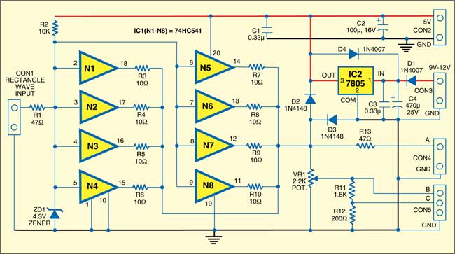
Potentiometer VR1 is used to adjust the amplitude of the output signal on connector CON5. The amplitude of the output at terminal C is ten times lower than the amplitude of the output at terminal B. The amplitude of the signal output on terminal B is adjustable from ground up to the maximum provided by the integrated circuit. Zener diode ZD1 protects the input and diodes D2 and D3 protect the outputs of the circuit.
The buffer and driver for square-wave signals can have power supply from CON2 or CON3. At a time, only one of the two connectors is used to supply current. Connector CON2 is used to provide well-regulated 5V DC power supply. Connector CON3 provides unregulated 9V-12V DC power supply. The supply current depends on the IC used and is usually below 100 mA.
Assemble the circuit on a general-purpose PCB and enclose in a small cabinet. Fix the power supply connectors on the rear side of the cabinet and input and output connectors CON1, CON4 and CON5 on the front side. Also, connect potmeter VR1 on the front side for varying the output at terminal B of CON5. The circuit is now ready for use.