 Most kits with embedded microcontrollers (MCUs) operate off a single power supply (VCC) source like 5V or 3.3V. But for some experiments you need one or more positive voltages higher than VCC and one or more negative voltages lower than ground. Often, the required current is in several milli-amperes (mAs). In such cases, you may use ICL7660, ICL7660A or similar integrated circuits (ICs) for the power supply. But voltage and current provided by a single ICL7660 is not sufficient, so you may need two or more ICs in parallel or cascaded to meet the requirement. Presented here is a DC-to-DC converter module that is flexible and allows all basic configurations for ICL7660 and similar ICs.
Converter module circuit and working
ICL7660, MAX1044, ADM660, MAX660, MAX665, LTC1044, LTC1046 and some other similar ICs are DC-to-DC inductor-less converters. These ICs are not exact equivalents but have similar functions and are pin-to-pin compatible in many cases.
However, there are several important differences between them, including working frequency, maximal output current and power supply range. For example, LTC1046 can produce output current up to 50mA, ADM660 up to 100mA and ICL7660 up to 20mA.
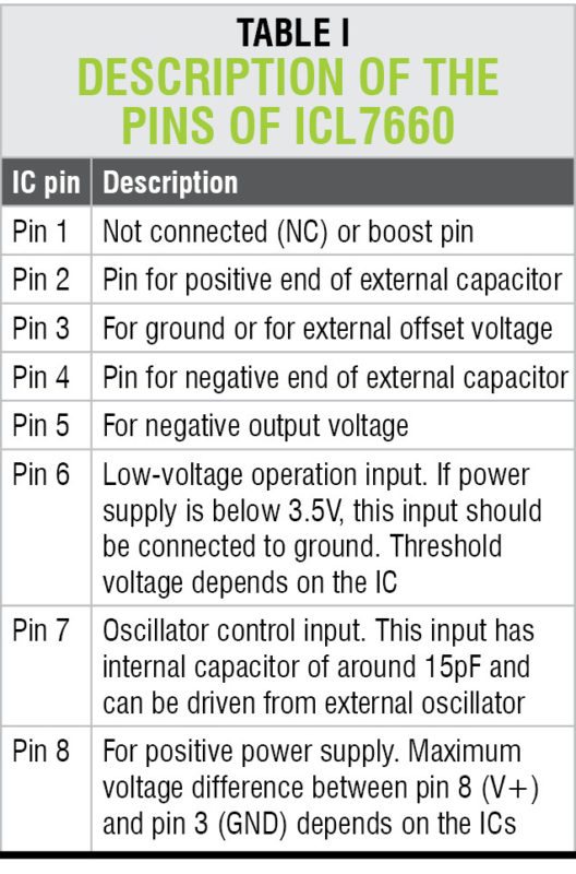
The proposed module will work with the ICs listed above and similar ICs but its performance will depend on the IC used. The mentioned ICs are available in 8-pin PDIP packages. Short descriptions of their each pin are given in Table I.
The ICs can work in several configurations. Input voltage can be inverted (VOUT = –VIN), divided by 2 (VOUT = VIN/2) or multiplied by n (VOUT = ±nVIN). The ICs can work with an internal or external oscillator.
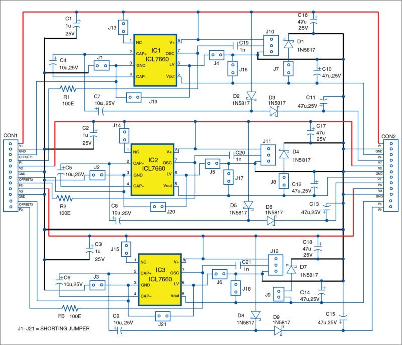
Fig. 1 shows the circuit diagram of the configurable DC-to-DC converter module using three ICL7660 ICs. The module has the following advantages:
1. IC1, IC2 and IC3 can be of same type or different.
2. Each IC can work with independent power supplies, namely, V1, V2 and V3.
3. Each IC can work in different configurations.
4. Outputs of the ICs can be paralleled for higher output current.
5. The ICs can be cascaded for higher voltages.
6. The ICs can work with external oscillators having the same or different frequencies.
7. Each module can produce single negative output voltage, approximately equal to –V1, –V2 and –V3 at V4, V5 and V6, respectively. That is,
V4 = –V1
V5 = –V2
V6 = –V3
8. Each module can produce single positive output voltage at V7, V8 and V9, respectively, which is approximately equal to:
V7 = 2×V1 – 2×Vd
V8 = 2×V2 – 2×Vd
V9 = 2×V3 – 2×Vd
Where Vd is the voltage drop across the corresponding Schottky diodes in series.
9. The module can produce positive and negative output voltages. All diodes (D1 through D9) should preferably be fast-switching Schottky diodes like 1N5817/8/9. BAT series, like BAT42, BAT43, BAT47, BAT48, but other similar Schottky diodes can also be used. While choosing these diodes, forward voltage drop and reverse voltage of the diodes should be taken into consideration.
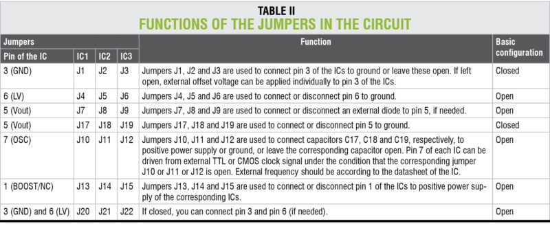
Jumpers. The ICs can be configured independently with several jumpers. Table II gives short descriptions of the functions of the jumpers used in the circuit.
Each IC has seven jumpers that permit it to implement almost all possible application circuits according to the datasheets of the IC. It is recommended to refer datasheets of the ICs before using the circuit.
Capacitors
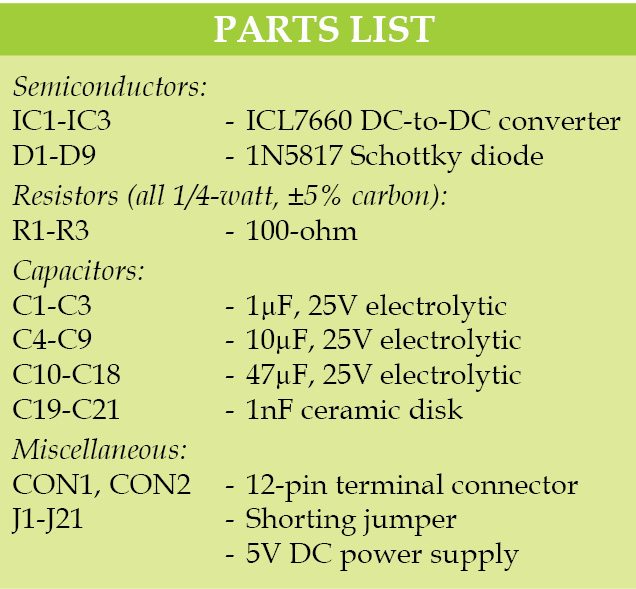
All capacitors in the circuit should work at high frequencies in switching power supplies. These capacitors depend on the ICs for working frequency and maximum output current, etc. Capacitors C1, C2 and C3 should be of 0.33µF to 1µF. Capacitors C4 through C15 are usually rated at 10µF to 100µF for 25V or more. Capacitors C16, C17 and C18 are of 47µF to 220µF for 16V or more. Capacitors C19, C20 and C21 determine the frequencies of internal oscillators. These capacitors can have any appropriate values but the usual values are between 0pF and 1nF.
Construction and testing
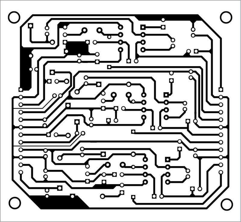
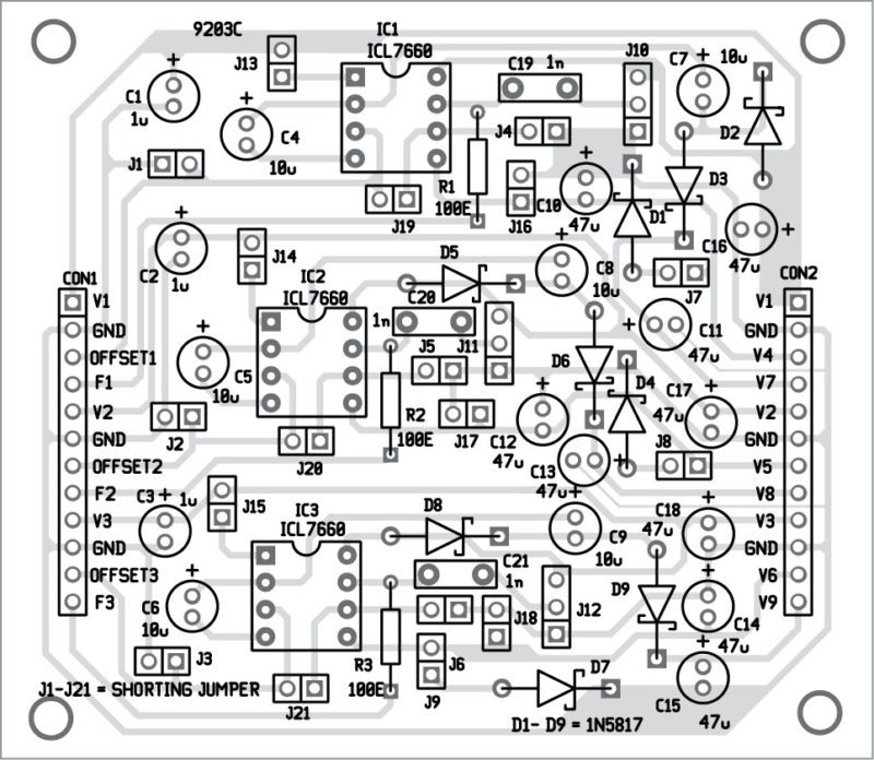
A single-side PCB layout for the configurable DC-DC converter module is shown in Fig. 2 and its components layout in Fig. 3. After assembling the circuit on a PCB, enclose it in a suitable cabinet with connectors CON1 and CON2 fixed on the front panel. Input voltages and frequencies (F1, F2 and F3) are applied to CON1 and outputs are taken from CON2.
Download PCB and component layout PDFs: click here
After proper assembly and configuration with jumpers, the circuit will start working immediately when power is supplied. It has a lot of advantages. For instance, voltages V1, V2 and V3 can be the same or different, and outputs can be paralleled for higher output current.
Petre Tzv Petrov was a researcher and assistant professor in Technical University of Sofia (Bulgaria) and expert-lecturer in OFPPT(Casablance), Kingdom of Morocco. Now he is working as an electronics engineer in the private sector in Bulgaria


