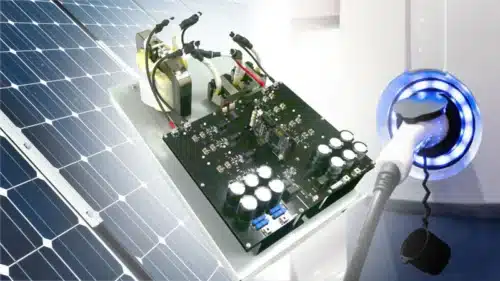
The design uses SiC MOSFETs and dual active bridge topology, suitable for power applications like electric vehicle charging and solar inverters.

Addressing environmental and energy challenges is a pressing global concern, especially as the demand for electric power surges alongside a growing emphasis on energy conservation and the need for highly efficient, compact power conversion systems. In response to escalating global warming gas emissions, numerous developed and emerging countries like China and India are implementing regulations to phase out gasoline vehicles. This trend underscores a global shift towards adopting electric vehicles (EVs) to diminish reliance on gasoline. However, transitioning to EVs presents challenges, particularly in developing robust charging infrastructures, which are deemed a critical hurdle. Concurrently, there’s a rising global demand for solar power generation systems centred around efficient power conversion circuits that effectively manage battery storage and energy supply to the grid. Toshiba has launched a 5kW Isolated Bidirectional DC-DC Converter reference design to address this challenge. It demonstrates how to enhance the efficiency of power supply designs using SiC MOSFETs.
The design employs the Dual Active Bridge (DAB) topology, a favoured approach for high-power converters, which features full bridges on both sides. These bridges enable control over the power’s direction and quantity by modifying the phase difference between the circuits on the left and right sides. As a highly adaptable reference design, it is an excellent foundation for developing and prototyping applications that require robust power conversion, such as electric vehicle charging stations and solar power inverters.
The DAB method, utilised in the reference design, employs full bridges on both sides to control the direction and amount of power transmission by adjusting the phase difference between the left and right bridge circuits. This reference design highlights several key features: it facilitates bidirectional high-power conversion using the DAB method, which is chosen over other power topologies to emphasise efficiency. The DAB method’s full-bridge configuration on both the high- and low-voltage sides allows for higher power handling than the half-bridge method. It enables soft switching through phase-shift power transfer, resulting in higher conversion efficiencies. While insulated gate bipolar transistors (IGBTs) traditionally suffer from significant switching losses, adopting silicon carbide (SiC) MOSFETs in this design achieves high power conversion and enhanced efficiency levels.
The reference design achieves high conversion efficiency using the DAB bidirectional DC-DC conversion method, combined with SiC MOSFETs as the switching elements. A critical advantage of SiC MOSFETs is their ability to operate at higher switching frequencies than IGBTs, significantly enhancing the performance and efficiency of power conversion circuits. This has led to a widespread increase in the use of SiC power devices across a broad array of power-related applications.
Toshiba has tested this reference design. It comes with a bill of materials (BOM), schematics, assembly drawing, printed circuit board (PCB) layout, and more. The company’s website has additional data about the reference design. To read more about this reference design, click here.


