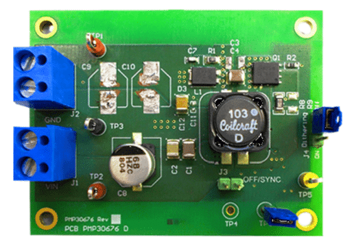
The reference design for automotive SEPIC converters enhances modulation with a sinusoidal output of up to 120 Hz, simplifying complex design processes.

Discontinuous Mode (DCM) in a Single-Ended Primary Inductor Converter (SEPIC) with a modulated output voltage is particularly advantageous for applications in automotive and industrial systems where efficiency, adaptability, and reliability are paramount. Employing DCM allows the converter to maintain high efficiency across varying loads and supply conditions, enhances component longevity by reducing stress, and simplifies the control loop. Moreover, it improves transient responses, reduces electromagnetic interference, and supports a wide input voltage range. These benefits make DCM SEPIC converters with modulated outputs highly effective for stable voltage regulation in dynamic and demanding environments. Texas Instruments (TI) has launched a discontinuous mode SEPIC reference design with modulated output voltage to simplify the design process.
The automotive single-ended primary inductor converter (SEPIC), utilizing the LM5156-Q1 or LM51561-Q1 devices, is specifically designed to support a modulated output voltage featuring a sinusoidal waveform of 60 VPP at up to 120 Hz. The design encounters certain dynamic limitations when operated in different modes. When operating in continuous-conduction mode (CCM), it is dynamically limited by the right half plane zero (RHPZ). Additionally, using non-synchronous rectification at low output voltages can lead to reduced discharge current at the output capacitor by the resistive load, causing the output voltage to no longer follow the desired modulating waveform.
To address these challenges, the magnetizing inductance is minimized to allow the power stage to operate in discontinuous mode (DCM), which effectively shifts the right half plane zero (RHPZ) beyond 300 kHz under the worst-case scenarios of the lowest input voltage and maximum load. However, the performance of the system is still limited by the gain bandwidth of the error amplifier and the Nyquist criteria. With a loop bandwidth of 10 kHz, this design is capable of adequately managing only 100 Hz at the output. The DCM approach significantly reduces Qrr ringing at the semiconductors and decreases the size of the dual inductor.
Despite these improvements, the converter generates a high ripple current, which in turn leads to magnetizing losses, alternating current losses at the winding, and a significant output ripple voltage. Nevertheless, these disadvantages are acceptable for applications requiring a maximum output power of just 18 W. One practical application of this technology is in smart glass modules, where precise power modulation and management are crucial.
Features of the design include a loop bandwidth of 10 kHz for optimal dynamics, enabling modulation of the output voltage up to a frequency of 120 Hz with a sinusoidal waveform. Additionally, this reference design has been fully constructed and rigorously tested in a laboratory setting.
TI has tested this reference design. It comes with a bill of materials (BOM), schematics, assembly drawing, printed circuit board (PCB) layout, etc. You can find additional data about the reference design on the company’s website. To read more about this reference design, click here.


