 Many single-ended analogue signals do not have DC components or appropriate DC offsets. Due to that, these require very high input resistance for analogue-to-digital converter (ADC) inputs. This simple universal dual level shifter and buffer for AC and audio signals can be used for ADCs, MCU kits and Arduino. It does not need any special adjustment to work properly. Before using the circuit, select and adjust the appropriate DC offset for each operational amplifier, every time.
We need analogue level shifters and buffers between the source of analogue signals (AC or audio) and inputs of the ADC. Here, we see a simple solution for two channels of the ADC. The circuit can be multiplied for any number of ADC inputs.
Circuit and working
Circuit diagram of the dual and audio level shifter and buffer for ADCs, MCU kits and Arduino is shown in Fig. 1.
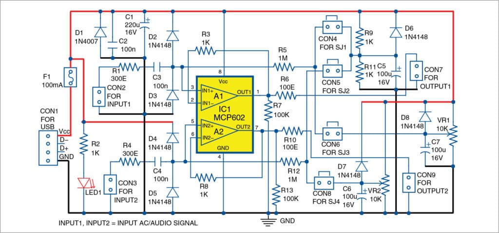
The circuit has two analogue channels. In each channel, there is a single operational amplifier working as a level shifter and buffer follower. Input AC or audio signal is applied to input1 and input2. Input resistance at low frequency is around 1-mega-ohm. Bandwidth of each channel is 2Hz to more than 100kHz.
Capacitors C3 and C4 cut the input DC components (if any). Resistors R1 and R4 and diodes D2 through D5 protect the inputs of operational amplifier IC1. Resistors R5 and R12 are used to apply the DC offset to the input of op-amps A1 and A2. For each op-amp, there are two independent options for the DC offset. First is fixed offset, which is equal to Vcc/2. Second is adjustable offset.
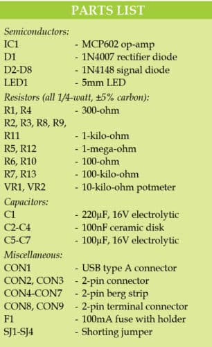
The table gives the selection of the DC offsets for the level shifters with shorting jumpers.
Shorting jumpers SJ1 and SJ2 should not be closed at the same time. Similarly, SJ3 and SJ4 should also not be closed at the same time. The circuit is operational in full power supply range of the op-amps. Use rail-to-rail input and output op-amps.
Construction and testing
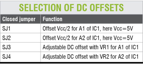
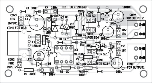
A PCB layout for the dual level shifter and buffer is shown in Fig. 2 and its components layout in Fig. 3. After assembling the circuit on the PCB, connect the USB connector for 5V (VCC) regulated power supply. Connect potmeters VR1 and VR2 on the front panel of the cabinet for variable offsets. Connect LED1 on the front panel to indicate power status. Use shorting jumpers according to requirement, as shown in the table.
Download PCB and Component Layout PDFs: click here
Petre Tzv Petrov was a researcher and assistant professor in Technical University of Sofia, Bulgaria and expert lecturer in OFPPT (Casablanca), Kingdom of Morocco. Now he is working as an electronics engineer in the private sector in Bulgaria.


