Data centres play a major role in expanding the enterprise computing capabilities. These are a centralised repository for storage, management and dissemination of data and information. Today’s central processing units (CPUs) are powerful and well-suited for high-level decision-making and control tasks, but their computing power cannot be scaled economically to keep pace with ever-increasing data centre requirements.
Hardware acceleration is a solution which may be implemented using a variety of technologies, including application-specific integrated circuits (ASICs), field-programmable gate arrays (FPGAs), graphical processing units (GPUs) and network processing units (NPUs). FPGAs are well known for their versatility. Many of these implement communication and control functions wholly, or in part, as soft intellectual property (IP). So in data centres FPGAs can play a role in cognitive computing, high-performance computing and the Internet of Things. These can serve as coprocessors to accelerate CPU workloads. This is an approach used in supercomputing and high-performance computing (HPC), done usually by teaming CPUs with Nvidia GPUs or Intel’s x86-based Xeon Phi coprocessors.
Cloud service systems are based upon processors. Software is driving the change, which extends beyond the rise of machine learning and training neural models. A whole new set of workloads is running in the cloud today, including virtualising networks, storage processing, compression and encryption. FPGAs slot into the standard server, drawing 25W from its PCI Express (PCIe) Gen 3 slot.

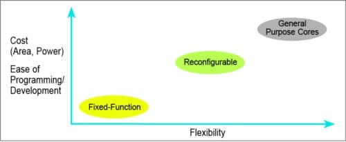
Fig. 1: Accelerator architecture

An integrated platform is one in which FPGA developers can upload their design in an IP library and data centre users can download the IP cores they need. This decoupling will enable widespread adoption of heterogeneous processing in data centres. Data centre operators can optimise the infrastructures by hyperscale, where FPGAs offer more sophisticated processing architectures that bring HPC-style parallel processing of workloads.

Fig. 2: Accelerator attach
Accelerator basics
Accelerating the data centre applications has become a requirement due to power and space constraints. Accelerators are needed to increase performance at a low total cost of ownership for targeted workloads.
An accelerator is a separate architectural substructure on the same chip or on a different die. It is architected with a different set of objectives than the base processor, where objectives are based on the needs of a special class of applications.
Accelerators are tuned to provide a higher performance at lower cost, or at lower power, or with less development effort than with the general-purpose base hardware. Depending on the domain, accelerators often bring greater than ten times advantage in performance, cost or power consumption over a general-purpose processor.
Examples of accelerators include floating-point coprocessors, GPUs to accelerate the rendering of a vertex-based 3D model into a 2D viewing plane, and accelerators for the motion estimation step of a video codec. Applications such as big data analytics, search, machine learning, network functions virtualisation, wireless 4G/5G, in-memory database processing, video analytics and network processing benefit from acceleration engines, which need to move data seamlessly among the various system components.
Coherent accelerators
HyperTransport, front-side bus (FSB) and QuickPath Interconnect (QPI) are not commercially successful because these have a proprietary ‘in socket’ attached, server mechanical fit challenges, need to give up processor socket, proprietary specification, licensing issues and always-lagging 6-12 month Cadence.
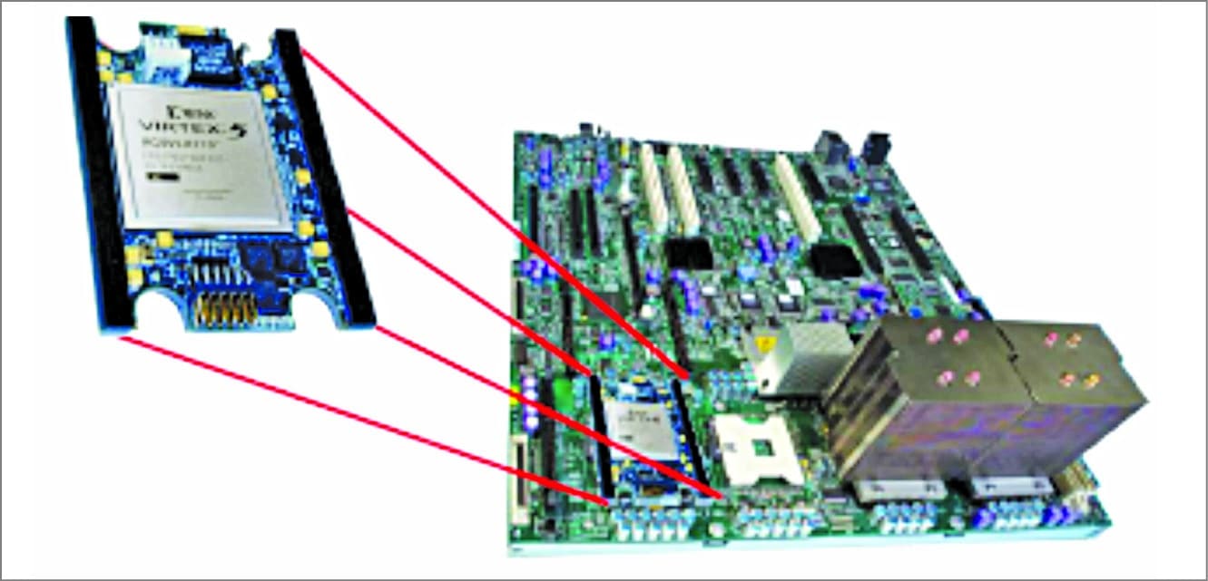
Fig. 3: ‘In socket’ coherent accelerators
IBM’s Coherent Accelerator Processor Interface (CAPI) interface resolves all these issues. This OpenPower-based solution is well documented and already commercialised. It has proprietary ‘in socket’ attached, and processors use all the available sockets. It is based on PCIe, hence there are no mechanical challenges. It is free, simple, OpenPower-licensed. Also, it is in sync with Power and Cadence’ PCIe interface IP.
Power9 processor
IBM’s next-generation Power9 processor will have 24 cores, double that of today’s Power8 chips. Design is optimised for two-socket scale-out servers (hence the name Power9 SO), and includes on-chip acceleration for compression and encryption.
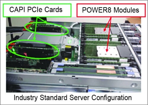
Fig. 4: Power8 modules with CAPI PCIe cards
Power9 will be available in two basic designs: a 24 SMT4 processor and a 12 SMT8 processor. The 24 SMT4 processor will be optimised for the Linux ecosystem and will target web service companies such as Google, which need to run across several thousand machines. It will feature four threads.
The 12 SMT8 processor will be optimised for the Power ecosystem and will target larger systems designed for running big data or artificial intelligence (AI) applications. It will feature eight threads.
Both designs will come in two models: The scale-out model will come with two CPU sockets on the motherboard, while the scale-up model will come with multiple CPU sockets.
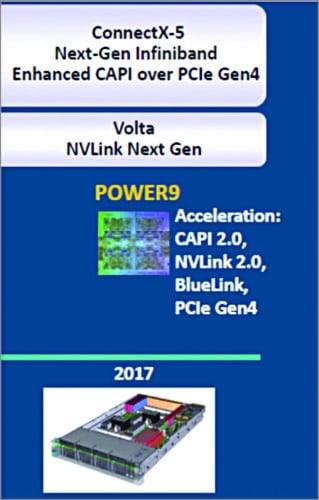
Fig. 5: Power processor roadmap
Power9 processor will be a 14nm high-performance FinFET product. It will directly attach to DDR4 RAM, connect to peripherals and Nvidia GPUs via PCIe Gen 4 and NVLink 2.0, and transfer accelerator data at 25Gbps speeds. Power9 processor will have multiple connectors to attach FPGAs, GPUs and ASICs. It will be well suited for AI, cognitive computing, analytics, visual computing and hyper-scale web serving. IBM will exclusively use Power9 in its servers and make it available to other hardware companies by licensing the design to them. Power9 processors can be attached directly to various accelerators rather than communicating via the PCIe bus.
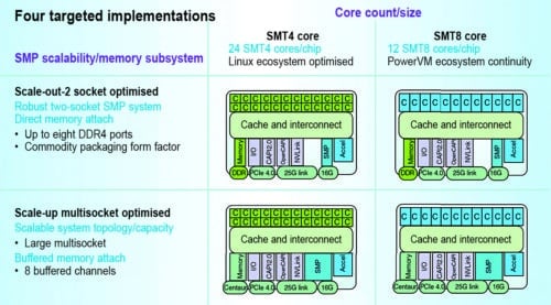
Fig. 6: SMT4 vs SMT8 core
Heterogeneous computing approaches for cloud data centres
In heterogeneous systems, different kinds of processors—x86 CPUs and FPGAs—cooperate on a computing task. Heterogeneous architectures are already widely used in the mobile world, where ARM CPUs, GPUs, encryption engines and digital signal processing (DSP) cores routinely work together, often on a single die.
There are two approaches to establish heterogeneous computing systems in cloud data centres.
The first approach is based on heterogeneous super nodes that tightly couple compute resources to multi-core CPUs and their coherent memory system via high-bandwidth, low-latency interconnects like CAPI or NVLink. CAPI is encapsulated by the PCIe and appears to use the same bus architecture with higher bandwidth capabilities and lower overall latencies. NVLink is a high-bandwidth, energy-efficient interconnect that enables ultra-fast communication between the CPU and GPU, and between GPUs. The technology allows data sharing at speeds five to twelve times faster than the traditional PCIe Gen 3 interconnect, resulting in dramatic speed-ups in application performance and creating a new breed of high-density, flexible servers for accelerated computing.
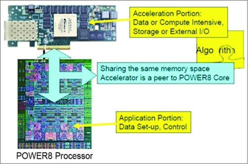
Fig. 7: CAPI FPGA accelerator (based on a standard PCIe accelerator)
The second approach is based on the disaggregation of data centre resources where the individual compute, memory and storage resources are connected via the network fabric and can be individually optimised and scaled in line with the cloud paradigm.
CAPI on Power9
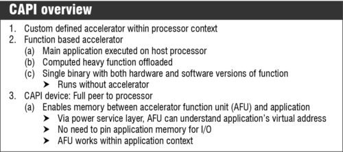
CAPI on Power9 system provides a high-performance solution for implementation of client-specific, computation-heavy algorithms on an FPGA. It can replace either application programs running on a core or custom acceleration implementations attached via input/output (I/O). Applications for CAPI include Monte Carlo algorithms, key value stores and financial and medical algorithms. CAPI removes the overhead and complexity of the I/O subsystem, allowing an accelerator to operate as part of an application.
A specific algorithm for acceleration is contained in a unit on the FPGA called the accelerator function unit (AFU or accelerator). AFU provides applications with a higher computational unit density for customised functions to improve the performance of the application and offload the host processor. Use of AFU allows cost-effective processing over a wide range of applications. CAPI can also be used as a base for flash memory expansion, as is the case for IBM Data Engine for NoSQL Power Systems Edition.
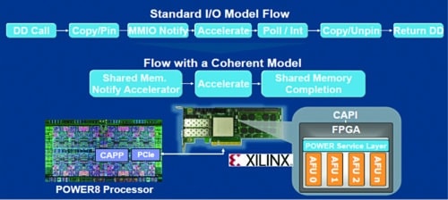
Fig. 8: Coherent accelerator processor interface
The Coherent accelerator processor proxy (CAPP) unit maintains a directory of all cache lines held by the off-chip accelerator, allowing it to act as the proxy that maintains architectural coherence for the accelerator across its virtual memory space. A power service layer (PSL) resides on the FPGA alongside the acceleration engine. It works in concert with the CAPP unit across a PCIe connection. The PSL provides a straightforward command to the client-written accelerator, which grants access to coherent memory.
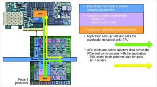
Fig. 9: CAPI technology connections
The CAPP and PSL handle all virtual-to-physical memory translations, simplifying the programming model and freeing the accelerator to do the number crunching directly on the data it receives. In addition, the PSL contains a 256kB resident cache on behalf of the accelerator. Based on the needs of the algorithm, the accelerator can direct the use of the cache via the type of memory accesses (read/write) as cacheable or non-cacheable. While the application executes on the host processor, the CAPI model offloads computation-heavy functions to the accelerator.
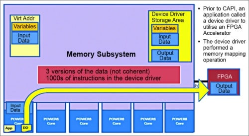
Fig. 10: Issues with PCI accelerators
The accelerator is a full peer to the application. It uses an unmodified virtual address with full access to the application’s address space. It uses the processor’s page tables directly with page faults handled by system software. For a CAPI solution, the application might set up the data for the AFU. The application sends the AFU a process element to initiate the data-intensive execution.
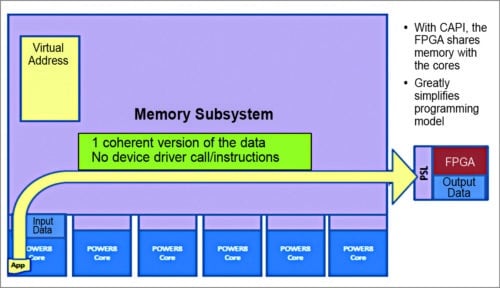
Fig. 11: Benefits of coherent accelerators
The process element contains a work element descriptor (WED) provided by the application. The WED can contain the full description of the job to be performed or a pointer to other main memory structures in the application’s memory space. The application can be the master or the slave to the accelerator—whichever mechanism is demanded by the algorithm. Alternatively, the accelerator can receive incoming packets from the network, work on the data, and then inform the application that the processed data is ready for consumption.

Fig. 12: Typical PCIe model flow
The acceleration platform can be integrated into cloud-based services. In this case, the application on the core runs as an Application as a Service (AaaS) for other applications that require services of the accelerator. The AaaS model maintains work queues for the accelerator on behalf of each of the requesting threads and performs any maintenance function needed to inform the accelerator of pending work. These connections are made through operating-system kernel extensions and library functions created specifically for CAPI.
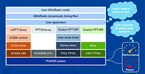
Fig. 13: FFTW (Fastest Fourier Transform in the West) on heterogeneous compute nodes
Operating-system kernel extensions will be made available to all Power-Linux Little Endian distributions starting with Canonical’s Ubuntu. When the system boots with a CAPI device connected on a PCIe port, kernel extensions recognise the CAPI device. These perform personalised system initialisations, including configuration of the CAPP unit connection to the PCIe port.
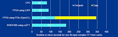
Fig. 14: Latency
Additional kernel extensions perform maintenance, system protection and communication functions. The client application uses a CAPI library called ‘libcxl,’ which provides multiple functions for the application to connect, call, communicate and disconnect with an available CAPI device. libcxl calls include many basic functions, such as those that allow the application to provide the virtual storage address of data structures to the accelerator. It also provides a memory-mapped I/O interface for the application to read/write registers in the accelerator’s register space on the FPGA.
Prior to CAPI, an application calls the device driver to utilise the FPGA accelerator. The device driver performs a memory mapping operation. CAPI connects a custom acceleration engine to the coherent fabric of the Power9 chip. Because FPGAs are reconfigurable, hardware can be customised without the traditional costs of hardware fabrication.
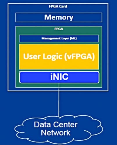
Fig. 15: Standalone FPGA accelerator
A standalone appliance/accelerator is equipped with an FPGA, (optional) local memory and an integrated network controller interface (iNIC).The iNIC enables the FPGA to hook itself to the network and to communicate with other DC resources, such as servers, disks, I/O and other FPGA appliances.
Part 2 coming soon…