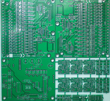
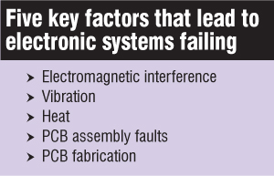
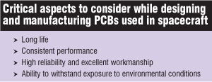
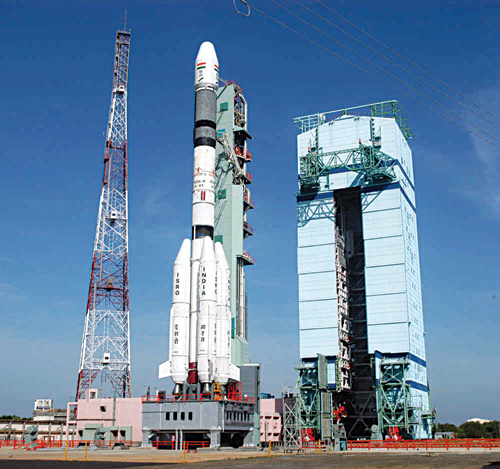
There is a high level of complexity involved whilst manufacturing PCBs, especially boards destined for military or aeronautical applications like spacecraft. There are certain procedures that have to be followed to create PCBs that work with high reliability in any environment. Let us find out more about these boards, the kind of environments spacecrafts operate in, the main characteristics to be measured while creating such PCBs and, finally, also look at the processes followed at the Indian Space Research Organisation (ISRO) to test them.
Why PCBs for space applications need to be top-notch?
About 70 percent of a spacecraft comprises electronics, and for any electronic device, the PCB is its backbone. It provides mechanical support for the electrical interconnections between components. However, when it comes to space applications, the process of manufacturing the PCB and ensuring its reliability becomes inherently complex.

PCBs targeted for aerospace applications are required to go above and beyond the standard processes and procedures in PCB design, fabrication, and assembly. In comparison to previous generations, designs for the military and aerospace sector today demand high reliability. In addition to a 100 per cent fault coverage using techniques such as design for test (DFT), the high RF and the thermal management require special attention with special PCB design and layout techniques.
System reliability plays an important role in spacecraft. Enormous effort goes into the making of a spacecraft, which is made up of a lot of sub-systems involving huge monetary investments. Besides, the users of the spacecraft have high expectations with respect to its performance, as it can cause human as well as material damage in case of a malfunction while in flight.
The components that populate consumer PCBs have tolerances anywhere between 5 and 10 per cent, whereas military or aeronautical standard components have tight tolerances of 1 to 2 per cent. These components are expensive but they are highly reliable, with gold-finish terminations, compared to components for consumer PCBs with tin-lead finishes. The components used for spacecraft cost about 5 to 10 times more than the commercial components.
Application-specific PCBs
Spacecrafts incorporate various types of PCBs—single-sided, double-sided and multi-layer boards, rigid flex boards, metal core boards for heat sink or thermal management purposes, and high-density interconnects for state-of-the-art components. Based on their applications, PCBs are classified into three general types—consumer boards, professional boards and high-reliability boards.

The most common applications are in consumer devices like radios, television sets, cellular phones and even testing equipment. These are called consumer boards. The materials used to make such boards are less expensive. In this case, the marketing factor is much higher than the reliability factor. It is not so important for the board to have very good and consistent electrical properties, since consumer devices are typically used and later discarded. Professional boards are used for technological developments where the reliability is the most important factor. Hence, when compared to the PCBs made for the consumer sector, these are made with much better quality material. Also, they have tighter electrical specifications and are fabricated using controlled fabrication techniques.
High-reliability boards are mainly used in the military and aeronautical sectors for strategic applications. These PCBs cannot afford to fail under extreme conditions and critical applications. They must provide the best performance, have extremely good electrical properties and a high-quality base material. They must be produced in a tightly controlled manufacturing process and should be able to work in harsh environments.
The different environments that spacecraft PCBs must operate in
PCBs in spacecraft basically experience three kinds of environments—ground, launch and the space environment. In the ground environment, i.e., during testing and fabrication, the PCB undergoes a lot of cleaning, thermal cycling, testing, soldering and other such processes. During the launch stage, there is heavy vibration due to the yawing and pitch spinning of the launch vehicle. Consequently, there is a lot of acoustic noise that is transferred to the structure of the vehicle, which is passed onto the electronic components. PCBs supporting such electronic packages should be able to quench the vibrations such that they are not transmitted to the components, causing damage to the leads.
These are important factors to be kept in mind while designing PCBs for launch vehicle programmes or any space programme. Once the launch is successful, the spacecraft has to withstand the forces of the space environment, which are much harsher than the ground or launch environment. The electronic packages incorporated on to PCBs used in spacecraft will face a lot of radiation and sudden changes in temperature.
Characteristics to be measured to ensure quality
Since it is virtually impossible to re-work on a PCB that has been manufactured, the process qualification plays a major role in ensuring a reliable PCB. Process qualification is basically an assurance of quality in manufacturing processes and testing methods. It confirms that products with pre-determined quality characteristics and attributes can be reproduced consistently within the established limits of the manufacturing process.
Mechanical aspects. It is important to measure the length, breadth and thickness of PCBs while designing them. Pitches are verified for mounting because once the components are mounted, the mechanical characteristics of the PCB cannot be altered. Warp and twist play an important role during assembly. Flexural strength, bond strength, peel strength, trace width, thickness, resolution, protective coatings (solder mask, solder coating, gold plating, etc), dielectric thickness, etch back, barrel regularity and annular rings are the other aspects that are verified before subjecting PCBs to environmental tests.
Electrical aspects. Intra-layer and inter-layer insulation checks are done because up to 14 layers are qualified for space applications. Hence, the intra-layer and inter-layer insulation resistances, dielectric withstanding capability and interconnection resistances play an important role. The current carrying capacity is another important characteristic to be measured.
After mechanical and electrical checks, the PCB is subjected to thermal shock cycling, solder-float tests and vibration tests. Long-term damping for humidity verification is done because the launch stations that the spacecraft are shifted to are typically located very close to the sea shore. The PCBs have to be well protected from the humidity point of view too. Hot and cold storage of PCBs is done, followed by vibration checks again. Lastly, a hot oil dip is done to find out if there is any lamination damage due to hot oil.
Some tests performed on spacecraft PCBs
Some of the tests that are performed on PCBs to ensure their high reliability are mentioned below, with a brief explanation on the purpose of each test.
Thermal shock cycling. The purpose of this test is to determine the resistance of a material, laminate or multi-layer board by repeated exposure to extreme temperatures for comparatively short periods of time. Interconnection resistance (ICR) is measured prior to and after thermal shock cycling. ICR must not change by more than 10 per cent of the initial value. Destructive tests like micro-sectioning are done to see whether the barrel or the plated through-hole is intact or not.
Thermal stress tests. This test is done to determine whether plated through-holes can withstand the thermodynamic effects of extreme heat to which they may be exposed during the assembly rework or repair process. The PCB is ‘baked’ at 125 to 150 degrees centigrade for six hours, after which it is subjected to six dips in the molten solder at 288 degrees centigrade, with a 120-second gap between the dips.

Vibration tests. This is an important event in the testing of PCBs because during vibration, anything can happen to the PCB. The interconnections are made through copper barrels that are coated inside the holes by chemical procees. Chemically deposited holes must be intact even after they are subjected to thermal cycling and vibration tests. The PCB is clamped on the ‘vibration table’ and sine input is swept ranging from 1 Hz to 2000 Hz. The resonance frequency is determined by mounting the transducer at the centre of the PCB. At the resonant frequency, the PCB is continuously vibrated for 30 minutes, after which the critical bare board test and micro-section is performed to observe any deformation in the barrels.
Humidity storage tests. This is to determine the effect of storage in moisture, which could result in a reduction in the performance of the PCB.
Other tests that are performed are out-gassing, dielectric withstanding voltage tests, insulation resistance tests, interconnection resistance tests, hot oil dip tests, peel strength tests, network simulation, bond strength tests, bare board tests and visual inspection.
An overview of the test pattern used for achieving high-reliability PCBs at ISRO
ISRO has an in-house PCB manufacturing plant that is called a ‘protoshop.’ For testing, 11 samples of a PCB are submitted to the quality assurance division, where engineers conduct Group-1 to Group-7 tests on them. These tests reveal the quality of the processes employed in fabricating the PCBs. Also, the tests check whether the process identification documentation and flow-chart has been made in a proper manner, whether non-conformance management has been recorded properly, and whether feedback from various in-line quality control (QC) at each stage of manufacturing has been recorded. After all the tests, the manufacturer of the PCB gets the information from ISRO’s QC.

In Group-1, pre-conditioning, cleaning and visual-eye examination are performed. The 11 samples or boards given for testing should have been manufactured in different batches. Out of 11, ten PCBs are subjected to destructive testing and one PCB is kept as a reference to note down the deviations after each test that the board undergoes.
In Group-2, the thermal cycling test is done, where the PCB is subjected to +125 to -55 degrees centigrade for hundred cycles. Similarly, after the thermal cycling is done, the test engineers carry out visual examination, bow and twist to check for continuity, inner layer IR checks, high voltage tests, peel strength, re-work simulation, and plating thickness, which is done by a micro-section. After each test that is carried out, the monitoring test is performed to check if anything has happened to the PCB during these tests.
In Group-3, the current carrying capacity for each trace design is fixed—this is one of the critical aspects to be measured, since the trace or copper track must not fail during operation. The board is also subjected to long-term damp heat to simulate various humidity conditions.
In Group-4, hot storage and cold storage tests are carried out. In the hot storage test, the PCB is subjected to a temperature of 85 degrees centigrade for 14 days, whereas in the cold storage test, it is kept for 24 hours at -40 degrees centigrade. A vibration test is also carried out to detect plated-through holes, especially in multi-layer boards.
In Group-5, high-temperature dip tests are done. Generally, when any re-work is done on PCBs, they are subjected to thermal excursion. Soldering and de-soldering of a component causes thermal excursion. This has to be verified by carrying out high-temperature dip tests. Generally, in any of the highly-reliable PCBs, the solder flow test is performed only once at 288 degrees centigrade for ten seconds, but for space-grade PCBs, the same test is done six times, i.e., the PCBs used for space applications are dipped in solder six times to see if plated-through holes, pads and other things are intact. This can be verified by performing the bow and twist test, peel strength test and micro-section of the PCB.
In Group-6, dimensional verification and solderability tests are carried out—for both hole and pads surface. These tests check if solder masks have been properly covered, because outerspace is highly contaminated with gases. Out-gassing of PCB materials is also checked.
Finally, Group-7 consists of the final tests that are carried out on PCBs. These tests check whether the components have been assembled properly on the PCB or not.
‘Reliability’ is the key word
In the world of defence and aerospace, reliability is very important. The fact that the systems used here are of national importance, and that they also have the potential to cause destruction to human life or property, is what makes safety such a high priority.
The author is a technical correspondent at EFY Bengaluru. This article is based on a talk by G.N.V. Prasad, manager, Printed Circuit Facility, ISRO, at the Electronics Rocks 2012 conference in Bengaluru


