The physical verification system is a trusted solution to enable users to achieve advanced node design signoff. It is efficient in reducing debug time, thus increasing productivity. The solution supports double patterning, advanced device extraction and 3D IC. It extends physical verification technology into design reliability checking and constraint validation. It also offers a distributed multi-threading processing capability and greatly accelerates throughput without requiring specialised hardware.
Biddle says, “Our experience with 20nm has shown this to be a real concern. Finding DPT violations late in the flow can have a significant effect on the design closure time. In addition, resolving DPT violation manually will be very time-consuming. A solution may not be obvious on looking at the violation.”

The Synopsys IC Validator incorporates a comprehensive range of techniques using a combination of property and equation based techniques to check conformity to foundry rules. By incorporating IC validation in-design, it provides a unified environment where the designer can avoid the potentially huge time lost in addressing issues like DPT rule violations detected late in the design process.
While many of the double-patterning rules could be built into place-and-route tools, implementation tools may not be able to see conflicts or rule violations at chip level or across hierarchical boundaries. Synopsys recommends fixing of physical violations at each step in the flow. IC Validator In-Design works natively with IC Compiler to ensure that these checks with many complex rules can be made very quickly to converge on sign-off closure efficiently.
A new, native hierarchical DPT colouring engine in IC Validator enables fast DPT decomposition analysis. The colouring engine makes it possible to accurately detect and quickly resolve DPT colour conflicts. IC Validator provides a mechanism for automatic detection and repair of DPT violation. In addition, the resultant GDSII for the chip will not be coloured, enabling the foundries to make optimal final decomposition choices. IC Validator’s in-design technology provides colouring information within the Milkyway database for parasitic extraction required for timing analysis and verification.
IC Validator In-Design is foundry-qualified and can also be used with both IC Compiler and Galaxy Custom Designer for physical verification of cell-based and custom circuits. Numerous 20nm tapeouts have already been completed using IC Validator for physical verification. The in-design capabilities along with IC Compiler help to shorten design closure time.
Kalra shares, “Increasing the number of masks and processing steps increases the marginality and variability in addition to increasing the manufacturing cost and time. It needs to be managed at the design level not only around transistors but at metal levels, requiring designers to take care of the local layout effects upfront during schematic designs with effective placement and routing. These device and metal variabilities need to be modeled in PDK, libraries and flow to have an effective signoff. With next-generation SoCs becoming multi-core with multiple interfaces and sensors, designers also need to understand the various sources of variability to exploit the technology options to its limits with appropriate EDA tools.”
3. Achieving higher levels of extraction and timing analysis
20 nm means accurate higher levels of extraction and timing analysis to allow manufacturing variability.
Ahuja informs that one new source of manufacturing variability at 20 nm is double patterning. Different masks on a given layer will often shift during the manufacturing process, resulting in variations that impact capacitance. Extraction software must take mask offset into account when extracting RC values.
Another source of variability is layout-dependent effects. At 20 nm, the layout context (what is placed near a device) can impact device performance by as much as 30 per cent. Thus circuit designers need to consider layout context as well as device topology, and simulate with layout effects prior to layout completion. This requires pre-layout sensitivity analysis tools, as well as context-driven placement and optimisation.
Biddle adds that as some of the critical routing layers in 20nm designs will be constructed out of two separate masks, there is a concern that shifts in alignment due to tolerances in the manufacturing process could lead to parasitic variations with resultant timing variations. One way to solve this variation is to add additional process corners to analyse. However, this will have a potentially huge impact on design turnaround time and is therefore not a preferred solution.
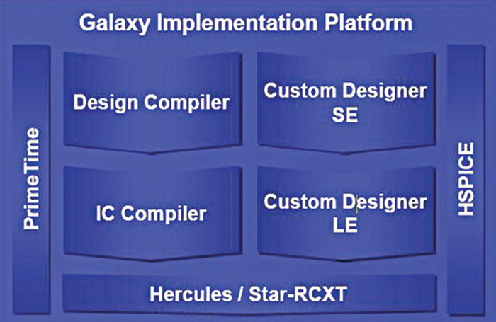
“While the full impact of this will not be known until the industry has gained more experience and the foundries optimise their manufacturing techniques, we have built a foundry-recommended capability into our extraction and static timing analysis tools StarRC and PrimeTime in case it is required,” he added.


