Here is a comprehensive guide to making your own PCBs at home using materials that are readily available in shops and online stores. While it addresses single-sided PCBs, it can be extended to create double-sided PCBs as well. The steps involved in making single-sided PCBs, in that order, are:
- Create a schematic
- Create a PCB layout
- Create the artwork
- Transfer the artwork onto the PCB laminate; let’s call this stage ‘artwork transfer’ or
- ‘exposing the PCB’
- Mask the area where you want to retain copper. This stage is called ‘developing’
- Remove copper from the PCB laminate where you don’t want it, e.g., tracks, etc. This process is called ‘etching’
- Remove the masking material to reveal the PCB
- Drill holes to solder and mount components and accessories or sub-assemblies. This stage may not be required if the PCB is being prepared for surface-mount components
- Tin the copper tracks to avoid oxidation of copper
- Deposit some sort of protective material on the side of the PCB that contains copper tracks, also called ‘solder side.’ This material does not allow solder to stick to the copper tracks other than where solder needs to stick, like component pads. This process is called ‘masking’
- Print the ‘silkscreen’ on the components side of the PCB to mark the component references corresponding to the components in the schematic
This article detail steps 1 through 8 as these are sufficient for most applications and can be performed at home.
However, your project circumstances and requirements will determine the steps that you need to perform. For example, if the artwork is already available, you may skip steps 1 and 2 and jump to step 3.
Step 1: Create a schematic
The prerequisite for this step is that the circuit for which you want to create the schematic is available along with component details like values, power rating and package details (size of the component, the spacing and layout of its connecting pins, etc). If that’s not the case, you may consider using some kind of simulation software like LT Spice or Proteus to draw the schematic and perform simulation on it. This may save you both time and money as:
1. Experimenting and reworking of a software simulated model is far less time consuming than procuring all the components that would be required for designing your circuit
2. You need not buy the components till you simulate and check everything theoretically to a large extent on the software.
If the components are handy, you may even use a general-purpose breadboard to quickly wire the circuit and test it. So let’s say that you have the circuit for which we wish to create the schematic. At this stage, you may want to consider using some kind of software tool for drawing the schematic on the computer. As you will soon realise, there are several advantages to using this tool as it works well beyond merely as a drafting or drawing aid. Eagle CAD, in particular, is extremely useful as it helps you create great schematics and much more. Its free version has some limitations like the maximum PCB size (board size) of 10x8cm2 and only two signal layers allowed. Even with these limitations, the tool is sufficient for most constructional projects.
Eagle comes with loads of goodies like a huge device library, several third-party libraries from manufacturers, built-in scripts that can perform many critical static checks, generate bill-of-materials and Gerber files that can be sent to a PCB manufacturing house, and much more. You can find loads of information and tutorials on YouTube and other web resources about Eagle CAD and similar software tools. Note that Eagle tool is used here for illustration purpose only, and you may use any other suitable tool of your liking, like Proteus.
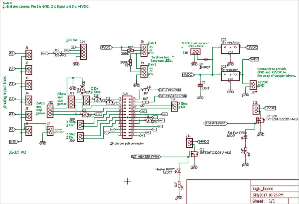
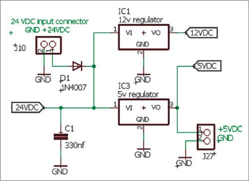
By now you should have a schematic like the one in Fig. 2. Here Fig. 3 is a close-up of the top right corner of Fig. 2. Eagle also provides a very useful feature called ‘electrical rule check’ (ERC), which can be used to test schematics for electrical errors and warnings. You will be surprised to see the number of warnings and errors reported by the tool for the schematic that you prepared and thought was perfect.
Step 2: Create a PCB layout of the schematic
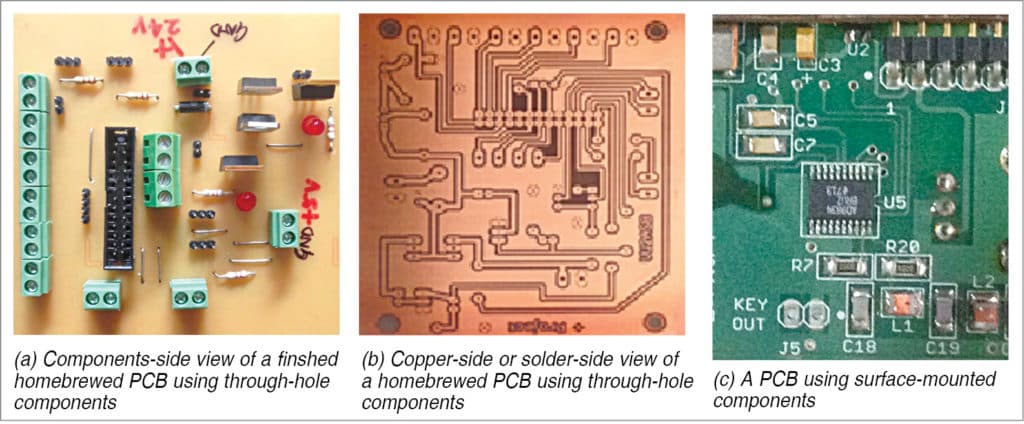
You may choose to use either through-hole components or surface-mount components (see Fig. 1), or a combination of both. This step remains the same for both types of components, except that some extra precaution needs to be exercised for through-hole components. Many software tools like Eagle allow you to import all the components from the schematic created by you to the board layout view while concurrently validating the board layout view (aka board view) electrically against the schematic. In this view, the board boundary is displayed, with all the components placed outside it, to begin with.
You can then start placing components within the board boundary by dragging them, one at a time. All the components show lines called ‘airwires‘ to display the electrical connectivity between their pins and pins of other components they connect with. This ensures that you do not miss out on any electrical connection inadvertently. By the end of this step, no ‘airwires’ should be visible and the board layout should be complete.
Eagle also provides the design rules check (DRC) feature, which checks the board against a set of predefined design rules. You will find similar features in other tools as well.
Tips, pitfalls and workarounds
If you use through-hole components, you need to drill holes for the component leads (step 8). A popular choice for drilling holes is a mini-push-type hand-drill machine as shown in Fig. 4. The bit normally used to make through-holes in the PCB has 1mm Dia. These drills are fine for 40-pin DIL header (Fig. 5) and drilling holes for components like resistors, capacitors and transistors, where a degree of misalignment is acceptable because you can handle it at the time of mounting components. However, it is very difficult to drill multiple holes perfectly in a straight line with exactly the same spacing (usually 2.54mm), like dual-line pins of an IC (see Fig. 13) or a header block (see Fig. 5), without any alignment error. And it is highly likely that you will end up in the situation shown in Fig. 6.


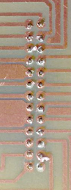
You will notice that the drill hole almost consumes the entire component pad, leaving no copper on the pad to hold any solder to bind the track connected to the pad with the component lead. This happens for a number of reasons:
1. The quality and precision with which a hole can be drilled by the mini push-drill (shown in Fig. 4) leave a lot to be desired. Typically, for PCB application the minimum prescribed speed is 25,000rpm, which may go up to 200,000rpm for multilayer micro vias, whereas manually operated hobby mini push-drills operate at a very low rpm and wobble
2. Most PCB laminates are made of fibreglass or glass epoxy, which are abrasive materials and wears away steel bits really fast. One solution is to use solid tungsten carbide bits, which last about ten times longer than steel bits. Unfortunately, these bits can’t be used with mini-push-drills as they are very brittle and break with the slightest change in the angle of contact
3. It is virtually impossible to keep the drill absolutely perpendicular to the PCB at all times while pushing the plunger of the drill axially up and down
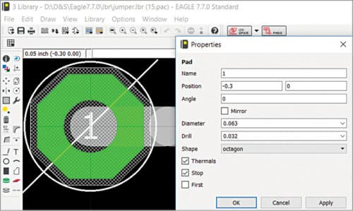
Commercial PCB manufacturing houses have appropriate manufacturing equipment that addresses the above three aspects. Eagle and most other software solutions use default parameters like pad diameter and shape (see Eagle default pad size and shape for jumpers in Fig. 7), which can be realised by commercial PCB making houses. For home brewing PCBs you need to work around these limitations. One way to do this is to use a bigger component pad size, but here is a trade-off: If you use very big pad size, you may end up having solder bridges across the component pads. If the pad size is too small, the drill hole may occupy the entire pad leaving no copper to solder on.
What parameters you use is also a function of the component type. Here we consider three types of components: discrete two-legged components like resistors, capacitors, transistors and jumpers; connectors like header blocks that have single-in-line or dual-in-line pins; and integrated circuits (ICs). These tips can also be used for other components with care and caution.
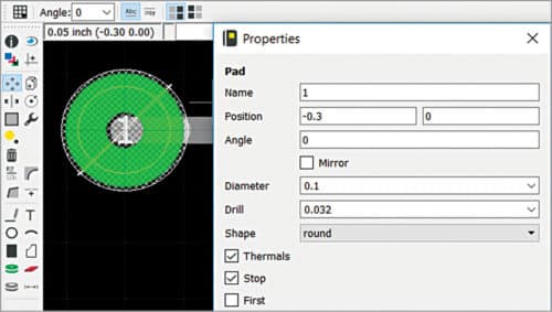
For discrete two-legged components, examine Fig. 7 for the default pad size and shape used by Eagle for jumpers. Fig. 8 shows the recommended pad size and shape for jumpers. These specifications can also be used for through-hole components like resistors, capacitors and transistors. The recommended diameter is 0.1 inch and drill size is 0.032 inch. Drill size may be reduced to 0.027 inches. Though this drill size is really small, it creates a very small drill centre in the pad, which is very useful for positioning the drill bit precisely in the centre of the pad. Use either round or octagon shape for pads.
For connectors like header blocks that have single-in-line or dual-in-line pins, refer to Eagle default pad size and shape in Fig. 9. Use the recommendations in Fig. 10 or Fig. 11. The two differ only in the pad shape. The recommendation is pad diameter of 1.9304mm (0.076 inches) and pad drill size of 0.7mm (0.02755906 inches). If you go overboard and use a larger pad size of 2.1844mm (0.086 inches) as shown in Fig. 12, you run the risk of having solder bridges between the pads.


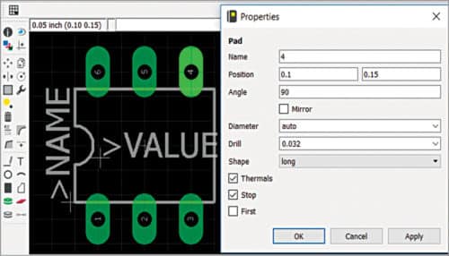
For ICs, see Fig. 13 for the default values used by Eagle and Fig. 14 for the recommended IC pad size and shape. The recommended pad diameter is 1.9304mm (0.076 inches) and pad drill size is 0.7mm (0.02755906 inches). Finally, check for electrical warnings and errors using the ERC and DRC capability of Eagle. Ensure that no air wires are left at the end of this step. The outcome should be similar to Fig. 16. The next step depends on the technique you choose for developing the PCB. I have used various techniques and found the one using positive-acting pre-sensitised PCB laminates the best.

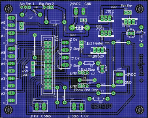
Its negative-acting pre-sensitised PCB variant requires a little different process for development. I chose the positive-acting board because it is easier to develop the artwork for it than for the negative-acting one. These boards can be bought online through many sources including eBay and Amazon.


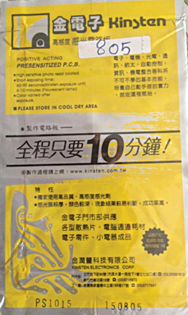
Initially, I used the single-sided glass-epoxy positive-acting pre-sensitised board from Ever-Muse with excellent results (see Fig. 19). More recently, I used a similar board, Kinsten type PS1015, which cost me around ₹ 250 a piece. The board specifications are:
- Dimensions: 10x15cm2
- Thickness: 1.6mm
- Material: Paper phenolic (PP), 1oz (35µm) copper foil, single side
- Exposure time: 6-10 minutes using a 20W fluorescent lamp placed 5cm above the PCB or 60 to 90 seconds using UV exposure box

I applied the process described in this article on the Kinsten PS1015 positive-acting pre-sensitised PCBs. The process will probably work as such with almost any similar board. It may need to be tweaked for optimal results if the board specifications are quite different.
Read Part 2


Is Instruments are available in INDIA for
Manufacturering of PCB ?
please tell me the software for PCB