


In the first part we touched base on multi-layer PCB design. In this part we discuss more about the same.
Multi-layer board and high-speed PCB design
A multi-layer board is a PCB having separate layers for power, ground and circuit tracks. It facilitates the use of entire copper layers for power and ground connections called power planes and ground planes, respectively. This decreases their inductance and impedance, allowing the use of cb high clock and signal frequencies and reducing ground noise. A rule of thumb is that, all other things being equal, a four-layer board will produce 15dB less radiation than a two-layer board.
New techniques employed in PCB design and manufacturing, on one hand, made it possible to drastically reduce the size of the PCB. On the other hand, however, clock frequencies have also increased dramatically, resulting in very fast rise times (or short edge rates) of clocks. Such short edge rates mean that decreased PCB dimensions have started to have significant effects on signal voltages and currents.

High-speed circuits are those circuits that use clocks of fast (or small) rise times. But how does one define high speed? Well, the term high speed is relative, where one is essentially comparing two speeds. Take clocks, for example. One of these two speeds is the rise time of the clocks, while the other is the speed of propagation of the electrons of the current that constitutes the clocks.
Now, the speed of movement of electrons in a PCB trace is less that the speed through air (which is the speed of light) since the field surrounding the electron has to travel through the PCB material that creates a drag. The equation given below gives the relation between speed of wave Vw along a PCB trace surrounded by PCB material to its speed C through a trace surrounded by air. er is relative permittivity of the PCB material.

Vw = C/√er
For example, speed of an electromagnetic field in a trace surrounded by air is about 30.5cm (12-inch) per nanosecond (hs). But when the trace is laid on an epoxy PCB (with er of 4), speed decreases to 15.2cm (6-inch) per nanosecond.
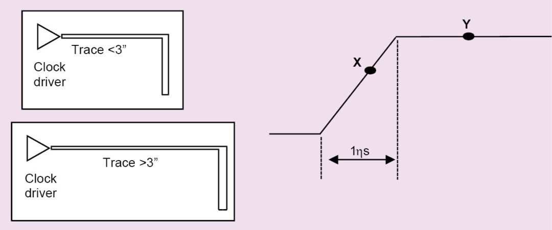
Now, consider a clock whose rise time is 1hs, and if dimensions of a PCB are greater than half the length traversed by this clock in 1hs (that is, greater than 7.6cm or 3-inch), track lengths will start to have significant effects on voltages. Let us see how.
Fig. 6 shows a typical clock with rise time of 1hs. In this time, current associated with this clock will travel 15.2cm (6-inch) along the track. Now, if the PCB dimension is less than 7.6cm (3-inch), reflected wave (wave will be invariably reflected if track changes direction or there is increase or decrease in track width) will arrive in less than 1hs (point X in Fig. 6), that is, at a time when the driver is still ramping the pulse up into the trace.
Because of driver inertia, reflected pulse will not have any effect on incident pulse. But if PCB dimensions (or track discontinuities) are greater than 7.6cm (3-inch), reflected pulse will arrive at point Y. Since driven clock is now stable, reflected pulse will have significant effect on incident clock.
Hence, for a PCB with dimensions greater than 7.6cm (3-inch), clock with rise times of 1hs will be considered high-speed and, for such cases, a radical design approach termed as high-speed PCB design using multi-layer boards will have to be followed.
Multi-layer concepts in Multi-Layer PCB Design
Let us take a look at some basic terms related to multi-player boards that we will be referring to time and again.
Board or layer stack-up. Stack-up is the name given to the order of various etched copper and dielectric layers that make up the board.
Power and ground planes. Multi-layer boards invariably use two layers of un-etched copper that are in the form of a continuous sheet, one for power supply (Vcc) and the other for ground (return), which are normally referred to as power and ground planes. Use of individual planes for power and ground lowers power distribution impedance and also reduces the signal-loop area. Hence, compared to a two-layer PCB, a simple four-layer PCB using such signal distribution can provide approximately 30dB improvement in EMC performance.
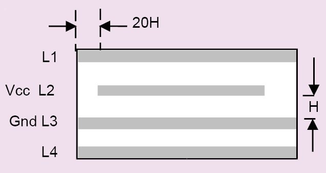
Reducing fringing fields: The 20H rule
Radio frequency (RF) currents between power and ground planes will cause emissions at the edges of planes. Such emissions are sometimes referred to as edge-fired emissions or fringing fields. These can be reduced by reducing the size of the power plane with respect to ground plane.
Ground plane dimensions [on layer 3 in Fig. 7(a)] should exceed power plane dimensions by 20H on all four sides, where H is the distance between power and ground planes. This will increase intrinsic self-resonant frequency of the PCB. Decreasing spacing between 0V and power planes also reduces fringing fields. Further decrease can be achieved by using a decap wall around the periphery of the power plane and inside the 0V plane periphery by 20H, where H is the plane pair spacing.
To read more about Multi-Layer PCB Design, turn to page 2
Reducing cross-talk: The 3W rule
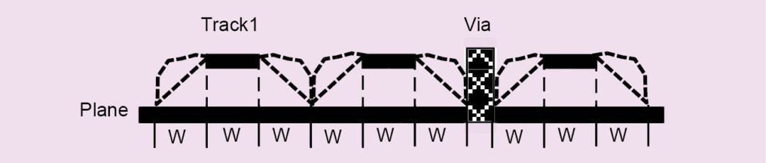
Cross-talk is capacitive coupling of signals from one circuit track to another. This can occur when a high-frequency track is running parallel to a susceptible track. Cross-talk flux and associated capacitive coupling can be reduced by 70 per cent if the two tracks are separated by a distance of 3W, where W is the width of the traces (measured from trace centre). This will cause track flux to terminate on the ground plane below rather than on adjacent tracks (shown as dotted lines in Fig. 8).
Guard traces in Multi-Layer PCB Design
Traces carrying high-frequency signals like clocks can cause coupling of clock harmonics on nearby traces, causing a jittering clock that can lead to problems elsewhere in the circuit.
These problems can be reduced by providing guard traces (Fig. 9) on either sides of such a track. Distance between the guard trace and the trace to be protected follows 3W rule.
Guard trace is connected to ground at both ends. If it is long, it should be connected to the ground plane at multiple points l/20 apart, where l is the minimum wavelength of the signal/clock.
Shunt trace in Multi-Layer PCB Design
This is a trace located immediately below the critical clock trace. It need not be connected to ground. Best isolation can be obtained by providing both guard and shunt traces, the former providing isolation by terminating magnetic field lines (shown as dotted lines in Fig. 9) and the latter providing isolation by terminating electric field lines.
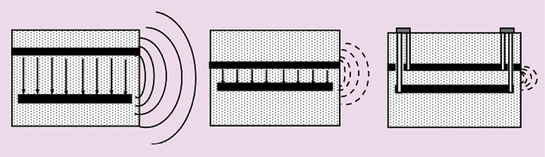
Image planes
An image plane is a plane physically adjacent (immediately below) to the signal routing plane.
It provides a low-impedance path for RF currents and reduces emissions since RF currents use the plane instead of air. Power supply and ground planes normally behave as image planes, although separate image planes can also be provided.
Via inductance
Each via in a board introduces additional inductance of 1hH and capacitance up to 0.5pF. Fig.
10 shows an equivalent circuit of a via; it consists of a series inductor and a shunt capacitor and, hence, acts as a low-pass filter. It can cause signal delays and affect the high-frequency performance of a board. Hence, vias should be reduced to a minimum.
Power and ground planes
A continuous sheet or foil of copper for ground (and power) can provide an infinite number of parallel paths and, hence, provide least-possible inductance. At higher frequency, skin effect also starts to play its role, causing an increase in resistive part of impedance.
A plane can provide a very large surface area and least-possible resistance. A ground plane therefore is the single-most cost-effective solution to reduce ground path impedance and solve most EMC problems.
To read more about Multi-Layer PCB Design, turn to page
Functions of a ground plane
Ground plane serves the following EMC and signal-integrity functions:
1. It has very low RF impedance and, hence, can provide devices and circuits with stable voltages at RF, which can be distributed evenly to a large number of devices and components by avoiding voltage drops.
2. RF return currents flow via 0V reference and, if a plane is used, return current can take whichever path it wants to, but prefers a path with lowest overall impedance (that is, one with least inductance and highest capacitance). So when a trace is routed over a ground plane, return currents will flow back right underneath the trace, reducing loop area enclosed by forward and return paths, thus reducing differential mode emission and susceptibility.
3. A plane underneath a track carrying high-frequency currents or a noisy IC will also behave as an image plane. As such fields emanating from the track or IC will be capacitively coupled to the image of the track in the plane rather than spreading out into space. This will reduce common-mode emissions.
4. Capacitive filters for blocking common-mode voltages are normally mounted between tracks entering the board and 0V reference. These bypass common-mode currents to ground, and a ground plane provides the ideal low-impedance path for these currents to ground.
Size of 0V plane
Size of a 0V plane must be such that it does not only lie beneath all components and traces of a circuit but also extends beyond these on all sides of the PCB by as much an amount as possible. This is because, although forward currents through a trace are constrained to flow in the trace, return currents flowing through a plane beneath the trace can spread out in the plane on either side of the trace. So edge of the ground plane should extend more than three times the trace-to-plane spacing (or three times the track width).
Openings and discontinuities in ground plane
Ground planes, as far as possible, should be continuous throughout. In a practical scenario, this is virtually impossible since anti-pads have to be provided in the ground plane. This causes the ground plane to be perforated, thus increasing its inductance. The situation can be controlled, first by restricting the urge to have tracks that change layers, second by optimising the size of anti-pads (<1mm) and third by using microvia technology, where anti-pads are largely eliminated.
Optimising anti-pad PCB design
Another issue with dense boards is that anti-pads should not merge with one another, otherwise these can create a larger opening that obviously hinders free flow of return currents and ruins the performance of the plane. In such cases, anti-pads’ dimensions and placement must be such that there is a web of 0V between these.
Connection of devices to planes
High contact impedance caused by improper connections of devices to 0V or power planes can be enough to compromise the low impedance benefits gained by using planes for 0V and power. Low inductance can be ensured by the following considerations:
1. Reducing the length and increasing width of the traces between pads and via connecting the component to 0V plane. The best way is to eliminate such traces altogether by using via-in-pad design.
2. Reducing the spacing between the 0V plane and the component, which will reduce the length of the via connecting the component to the plane, thus reducing via inductance.
3. Keeping vias carrying opposite currents as close to each other as possible to maximise their mutual inductance.
Position of devices
Digital ICs and crystals are known to generate intense near-fields in their immediate vicinity that can radiate, causing common-mode noise generation and coupling to nearby traces. This spread can be reduced by using an unbroken ground plane on the immediate bottom layer of the noisy component, which serves as an image plane terminating the radiated fields.
If the ICs are located near the edge of the PCB, 0V plane will be only on one side of the IC and the fields can radiate from the other side. Hence, noisy ICs and crystals should never be located on the edge of the PCB. As a general rule of thumb, ICs carrying digital signals with rise time of two nanoseconds or analogue components with frequencies more than 200MHz, should have an unbroken plane that extends at least 5mm beyond its periphery.
To read more about Multi-Layer PCB Design, turn to page 4
Layer stacking in boards
Layer stackup in a PCB is an important factor in determining the EMC performance of a product. While deciding the order in which various layers are stacked, following objectives must be kept in mind:
1. A signal layer should always be adjacent to a plane and be tightly coupled (close) to it. This reduces the loop area enclosed by forward and return signals.
2. Power and ground planes should be closely coupled together to maximise decoupling capacitance and to reduce ground noise.
3. High-speed signals should be routed on buried layers located between planes. In this way, the planes can act as shields and contain the radiation from high-speed traces.
4. Multiple ground planes are very advantageous, since these will lower the ground (reference plane) impedance of the board and reduce common-mode radiation.
All the above objectives can be met if one uses an eight-layer board. On four- and six-layer boards, objectives 2 and 3 are not achievable and a compromise has to be reached, although multiple ground planes can be provided on a six-layer board, at the expense of a signal layer.
Board stacking for four-layer boards. There are two conflicting considerations while deciding board stacking of four-layer boards. First is the separation between power and ground planes. The lower the separation, the higher is the decoupling capacitance, which can reduce the problem of supply transients and the associated generation of EMI.
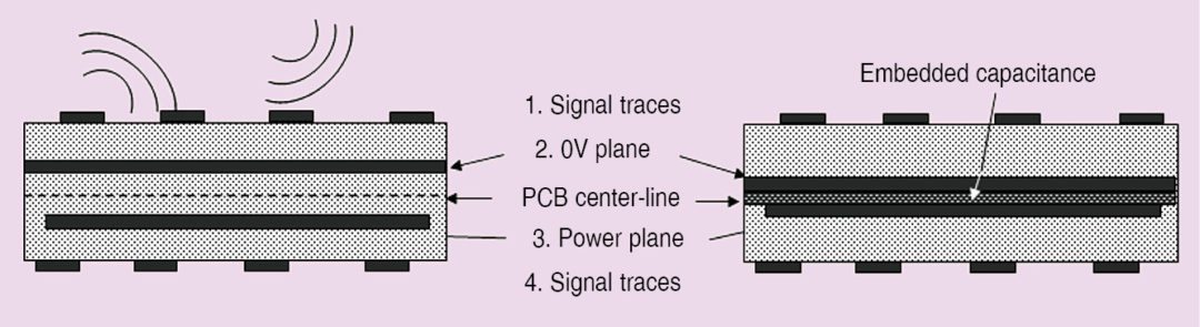
Second is the location of signal traces. Keeping power and ground planes closer means that signal traces have to be located on the outermost planes, which can cause increased emission and susceptibility. Fig. 13 shows a traditional stacking in a four-layer board where layers are spaced equally. Ground and power planes (layers 2 and 3) are sandwiched between signal layers (layers 1 and 4).
This type of distribution is called microstrip distribution and provides excellent decoupling capacitance between power and ground planes since these are located close together. This, along with reduced inductance, provides a 20dB to 30dB improvement for emission and susceptibility over the two-layer board. However, since traces are on the outside of the board, there exists potential emission and susceptibility.
To reduce potential emission and susceptibility problems of microstrip distribution, power and ground planes can be placed on the outside, while signal traces are sandwiched between the two. Such type of distribution is called stripline distribution. As shown in Fig. 14, signal traces on layers 2 and 3 are very close and are oriented perpendicular to each other (for reducing cross-talk). However, in this type of stacking, power and ground planes are so far apart and their distributed capacitance so low that there is negligible decoupling. This has to be compensated by providing larger decoupling capacitors.
Another drawback of stripline distribution is that of increasing difficulty as far as hand repairs and rework is concerned, especially during prototype development.
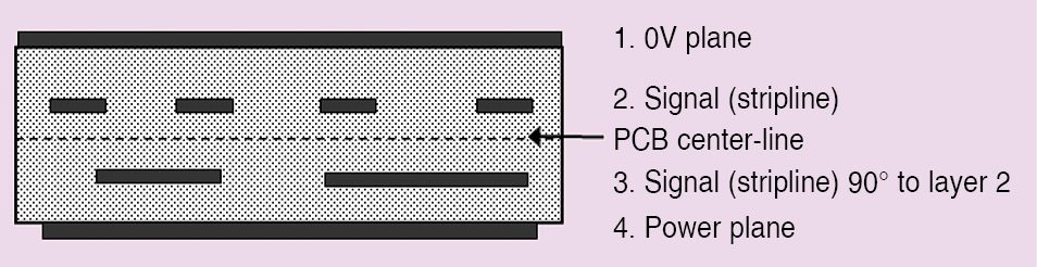
Board stacking of six-layer PCB. A six-layer board provides more PCB design options to improve EMC characteristics if stacking is done judiciously. Fig. 15 shows board stacking for a six-layer board. Here, power and 0V planes are located at the centre on either side of PCB centre line, with two signal-track layers above and below these. This type of stacking does not provide much EMC performance improvement over a four-layer board, except that there are just two additional signal layers to play with.
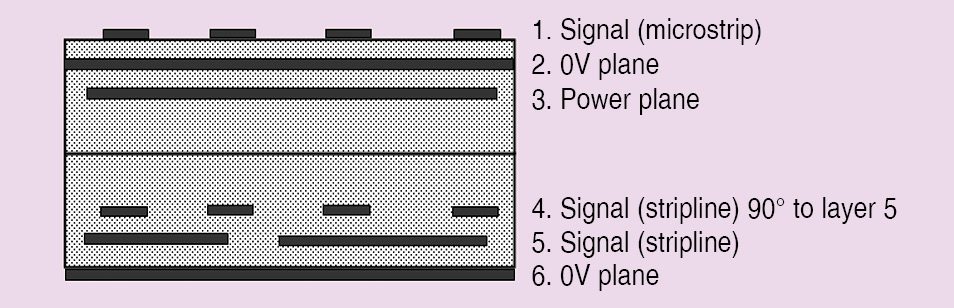
Some improvement in performance can be gained by using the type of stacking shown in Fig. 16, where positions of inner signal and power plane layers have been interchanged. This causes lowering of power supply decoupling, but can provide good shielding to high-speed signals if these are routed on the inner layers (layers 3 and 4). Again, tracks on these two inner layers have to be laid perpendicular to avoid cross-talk.
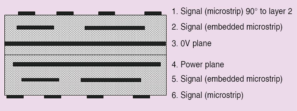
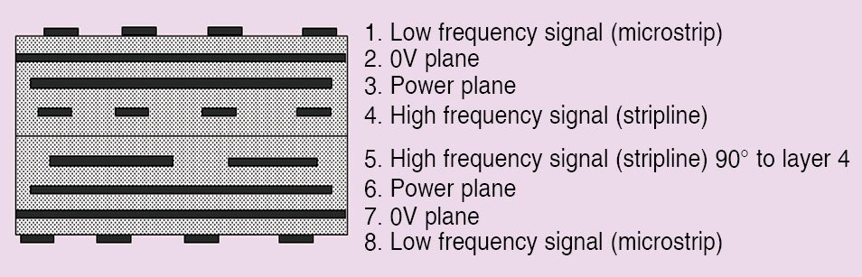
Board stacking of eight-layer PCB. Symmetrical stackup using an eight-layer PCB can meet all EMC requirements, without having to resort to compromises and additional efforts taken for unsymmetrical stackup. A traditional eight-layer symmetrical stackup is shown in Fig. 17, which consists of four signal layers and two pairs of 0V power plane. Since in both power plane pairs, 0V and power planes are located close together, excellent decoupling capacitance is obtained. Very good shielding can be provided by routing the high-speed, high-frequency tracks on innermost layers 4 and 5. Since the tracks on any layer have a plane nearby, image plane effect so created leads to low decoupling inductance. Overall, an eight-layer board provides the most-effective high-speed performance with 20dB or more improvement over a six-layer board.
Conclusion
So far we have discussed the various aspects of a good PCB design to take care of both signal integrity and EMI issues. A good PCB design is always the starting point of a good EMC design and is the most important too, since it reduces performance requirements of filters and shields, thus contributing a long way in reducing the product cost and keep the product competitive.
This article is an extract from a book by the author. The next part will cover grounding.
Chetan Kathalay is working as scientist in Electronics Test and Development Centre, Pune. He is BE in electronics from Nagpur University


“Now, the speed of movement of electrons in a PCB trace is less that the speed through air (which is the speed of light) since the field surrounding the electron has to travel through the PCB material that creates a drag.”
I can’t tell if you’re comparing (A) speed of electron through PCB trace to speed of electron through air or (B) speed of electron through PCB trace to speed of photon through air. Photons are the quanta for electromagnetic fields, so either you’re saying A and its wrong, or B and it was phrased poorly.