This article discusses what to expect from next-level field programmable gate arrays (FPGA Architectures).
Architectures of different field programmable gate arrays (FPGA) differ from vendor to vendor. Some vendors are Silego, Lattice Semiconductor, Xilinx, Microsemi and Achronix. Silego uses mixed-signal components. Whereas, Lattice Semiconductor is known for small form factors and ultra-low power FPGAs. Lattice Semiconductor’s iCE40UP3K FPGAs are designed for ultra-low power mobile applications, which include smartphones, tablets and other handheld devices.
Microsemi has SmartFusion2 system on chip (SoC) FPGAs. Altera and Xilinx FPGAs have great capacity and performance. Achronix Semiconductor’s asynchronous FPGAs operate at multi-gigahertz frequencies while consuming relatively little power. Achronix’s Speedcore embedded FPGAs improve throughput and latency performance by 10 times and reduce power by 50 percent and cost by 90 percent.

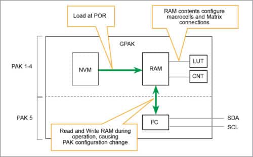
Silego FPGA
Silego announced its next-generation GPAK5 family, featuring a number of new and enhanced functionalities, including zero static-power asynchronous state machine (ASM) block, 8×8 scratchpad memory and I2C block. These new functions, along with configurable digital and analogue fabric seen in previous GPAK generations, are presented in a tiny 2.0mm x 3.0mm 20-pin STQFN package with 18 general-purpose inputs/outputs (GPIOs).
Lattice Semiconductor FPGA
The iCE40 Ultra Plus family includes integrated SPI and I2C blocks to interface virtually with all mobile sensors and application processors. iCE40UP3K features two-device density of 2800 range look-up tables (LUTs) with programmable IOs, which can be used as either SPI or I2C interface ports or GPIOs.

It also features 20 embedded block RAM memory blocks, 80 embedded block RAM memory bits, on-chip oscillators and four DSP blocks.
iCE40UP is available in a tiny form factor package—as small as 2.15mm x 2.55mm. It allows the device to easily fit into many applications. Typical applications include iCE40 Ultra devices, service LEDs, GPIO expanders, serial data IO level shifters and voice recognition for mobile applications.
Features include:
- 800 two-device logic architecture
- 40nm low power processors
- 100µA standby current
- 1024kb single-port SRAM
- Two IO pins to support I3C interface
- Two hardened SPI interfaces
- 24mA current drive RGB LED outputs
- 2.15mm×2.55mm ultra-small form factor
- On-chip DSP
- WLCS and QFN packages
Applications include voice-recognition applications, smartphones, tablets and consumer handheld devices, commercial and industrial handheld devices, multi-sensor management applications, sensor pre-processing and sensor fusion, sensor applications and USB 3.1 type-C cable detection/power delivery, among others.
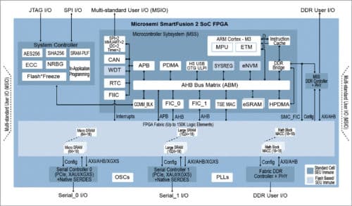
Microsemi FPGA
SmartFusion2 SoC FPGAs offer 5000 to 150,000 logic elements (LEs) with a 166MHz ARM Cortex-M3 processor, including ETM and instruction cache with on-chip eSRAM and eNVM, and a complete microcontroller (MCU) sub-system with extensive peripherals, including CAN, TSE and USB.
The architecture includes the following:
- Up to 16 high-speed transceiver lanes
- PCIe generation 2, XAUI/XGXS+, generic (EPCS) mode at 3.2G
- Up to 150,000 LEs, 5Mbit SRAM, 4Mbit eNVM
- Hard 667mbps DDR2/3 controllers
- Integrated DSP processing blocks
- Power as low as 7mW standby (typical)
- DPA hardened, AES256, SHA256
- On-demand NVM data integrity check
- SEU-protected/tolerant memories: eSRAMs, DDR Bridges
Achronix FPGA
Speedcore is the optimal hardware accelerator computation and communication infrastructure in data centres. Enterprises can no longer keep pace with exponential data growth rates, changing security and software virtualisation requirements. Traditional multi-core CPUs and SoCs need programmable hardware accelerators that pre-process and offload data to increase their compute performance.
In 2018, this centralisation is reaching its limit. Volume of data that will be needed to drive the next wave of applications is beginning to force a change in direction. Currently, only 10 per cent of enterprise-generated data is created and processed outside centralised data centres. Industry analyst Gartner predicts this figure will reach 50 per cent by 2022. This necessary reversal is driven by the shift towards hyper-connected cyber-physical systems, enabled by the arrival of technologies such as 5G wireless communications and a new wave of application-focused computing hardware.
Internet of Things (IoT) devices generate small individual amounts of data that are most efficiently aggregated and processed in large data centres. But as IoT devices and, increasingly, cyber-physical en-masse systems come to rely on the ability to interpret much more substantial data streams, the center of gravity needs to shift towards the edge. The automotive sector adopts changes that will be seen across many sectors.
Speedcore is the optimal solution for high-volume applications and offers significant advantages such as lower power, higher interface performance, lower system cost, higher system reliability and yields, and process technology to evaluate Speedcore. It is designed for computer and network acceleration applications, and is based on the same high-performance architecture.
Speedcore eFPGA products are fully supported by Achronix’s robust and proven ACE design tools. With Speedcore, customers specify optimal die size, power consumption and resource configuration required for their end application. They define quantity of LUTs, embedded memory blocks, DSP blocks, Speedcore aspect ratio and IO port connections. They can make tradeoffs between power and performance.
Achronix delivers GDS II of Speedcore IP to integrate directly into an SoC, and a custom, full-featured version of ACE design tools to design, verify and program the functionality of Speedcore eFPGA. Designers have long sought the inherent advantages that could come from embedding FPGA functionality as IP into SoCs for a host of different high-performance applications.
Achronix has now delivered eFPGA IP to customers who are developing high-performance computing products, where offloading compute-intensive functions from processors to FPGA IPs can provide a tremendous performance boost. While an exciting opportunity for Achronix, seeing FPGA IP become a reality is great news for the semiconductor industry, particularly considering the large market opportunity for compute high-performance applications.
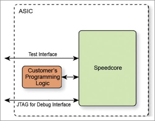
Speedcore eFPGA is an embeddable IP. It does not include programmable IO, and is designed to be surrounded by end-user ASIC.
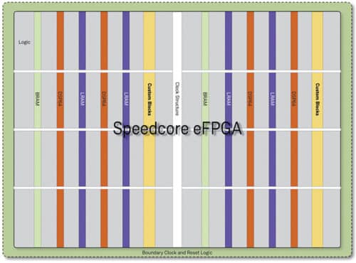
Speedcore is the optimal hardware accelerator
FPGAs are the optimal hardware accelerator solution, because accelerators need to be updated with new functionalities as algorithms are constantly changing. Standalone FPGAs are a convenient and practical solution for low- to medium-volume applications. Whereas, Speedcore is the optimal solution for high-volume applications and offers significant advantages, as given below.
Lower power. Speedcore has direct wire connections to the SoC, which eliminate large programmable IO buffers found in standalone FPGAs. Programmable IO circuitry accounts for half of the total power consumption of standalone FPGAs.
Speedcore is sized exactly to the requirements of the customer’s end application. The customer can tune the process technology to tradeoff performance for lower power.
Higher interface performance. Speedcore offers dramatically higher interface performance than standalone FPGAs in the form of lower latency. It is connected to the ASIC through an ultra-wide parallel interface, whereas standalone FPGAs typically connect through a high-latency serialiser/deserialiser (SerDes) structure.
Lower system cost. Speedcore die size is much smaller than standalone FPGAs, because the programmable IO buffer structure is eliminated.
FPGAs have high pin counts, which dictate the PCB layer count to support FPGA BGA package escape routing.
Additionally, Speedcore eliminates the need for all support components around the standalone FPGA, including power regulators, clock generators, level shifters, passive components and FPGA cooling.
Higher system reliability and yields. Integrating FPGA functionality into an ASIC improves system-level signal integrity, and eliminates reliability and yield loss associated with a standalone FPGA on the PCB.
Process technology
Speedcore is architected in modular fashion to support flexibility for customers to define their resource requirements, and for Achronix to rapidly configure Speedcore IP for delivery.
Additionally, the modular architecture allows Achronix to easily port the technology to different process technologies and metal stacks. Speedcore is available on TSMC 16FF+, and is in development on TSMC 7nm.
Evaluating Speedcore
Achronix’s ACE design tools include an example of Speedcore, where customers can compile their designs to evaluate Speedcore quality-of-results for performance, resource usage and compilation times.
Additionally, Achronix has complete documentation on Speedcore functionality and ASIC integration methodologies.
Physical integration with customer ASICs
Speedcore eFPGA is provided as a fixed-transistor-layout building block that integrates with industry-standard ASIC flows, such as Synopsys Design Compiler and IC Compiler. The following collateral is provided:
- Verilog definition of logical connectivity at boundary
- Liberty timing library for timing closure at boundary
- LEF defining physical floorplan, pins and metal blockages
- GDS/Oasis physical database
Xilinx FPGA
Xilinx has advanced architecture features like enhanced DSP slices incorporating 27×18-bit multipliers and dual adders that enable a massive jump in fixed- and IEEE standard 754 floating-point arithmetic performance and efficiency.
In addition, it has step-function increase in 3D IC inter-die bandwidth for virtual monolithic design, massive IO bandwidth and dramatic latency reduction through multiple integrated ASIC-class blocks for 100G Ethernet with RS-FEC, 150G Interlaken and PCIe generation 4, and static- and dynamic-power gating across a wide range of functional elements, yielding significant power savings.
Next-generation security with advanced approaches to AES bit-stream decryption and authentication, key-obfuscation and secure device programming, and DDR4 support up to 2666Mbps for massive memory interface bandwidth are additional features. Ultra-RAM provides massive on-chip memory for SRAM device integration, innovative IP interconnect optimisation technology for an additional 20 to 30 per cent advantage in performance/ per watt, MPSoC technology, combining soft and hard engines for real-time control, graphics and video processing, waveform and packet processing, and multi-level security, safety and reliability, and more.
Altera FPGA
Intel HyperFlex FPGA Architecture and Intel’s 14nm tri-gate process technology enable Intel Stratix 10 FPGAs and SoCs to deliver levels of performance and power efficiency that were unimaginable in previous-generation high-performance FPGAs. These devices deliver two times the core performance and five times the density compared to previous-generation Stratix V FPGAs.
In addition, these offer up to 70 per cent lower power than Stratix V FPGAs for equivalent performance, logic, internal memory and DSP blocks capable of 1GHz operation, embedded quad-core 64-bit ARM Cortex-A53 hard processor system (in SoC variants) and familiar FPGA design techniques supported by Intel Quartus Prime software.
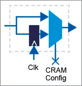
The centrepiece of Intel HyperFlex FPGA architecture is its registers design that adds bypassable hyper-registers to every routing segment in the FPGA core and at all functional block inputs. Fig. 5 shows a bypassable hyper-register, where the routing signal can bypass the register and go straight to the multiplexer, or go through the register first. The multiplexer is controlled by one bit of the FPGA configuration memory (CRAM).
Stratix 10 FPGA and SoC system integration includes heterogeneous 3D system-in-package integration, highest memory bandwidth with package, dual-mode transceiver with 56Gbps PAM-4 and 30Gbps NRZ, dual-mode transceiver with 56Gbps PAM-4 and 30Gbps NRZ. It has the highest density FPGA fabric with up to 5.5 million LEs, up to 10 tera floating point operations per second of IEEE 754-compliant single precision floating-point digital signal processing throughput, secure device manager with the most comprehensive security capabilities, integrated quad-core 64-bit ARM Cortex-A53 hard processor system up to 1.5GHz, and optimised and validated Intel Enpirion power solutions.
Stratix 10 devices are uniquely positioned to address the design challenges in next-generation, high-performance systems in virtually all end markets, including wireline and wireless communications, computing, storage, military, broadcast, medical, and test and measurement.
V.P. Sampath is a senior member of IEEE and a member of Institution of Engineers India, working in an FPGA design house. He has published international papers on VLSI and networks