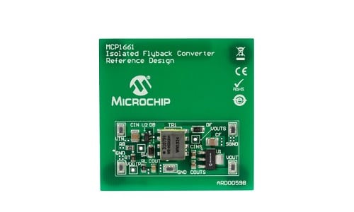
The reference design is for a DC-DC converter which employs a flyback topology and provides galvanic isolation thus making it suitable for sensitive applications.

Do you want to build your own DC-DC converter which is robust, efficient and safe for your sensitive equipments? Then this reference design from Microchip will help you build your isolated flyback converter that can take input from a USB output and provide a constant and reliable output.
The MCP1661 Flyback Converter Reference Design from Microchip is an isolated flyback converter that offers galvanic isolation. The MCP1661 is a constant Pulse-Width Modulation (PWM) frequency boost (step-up) converter, based on a Peak Current mode architecture which delivers high efficiency over a wide load range from two-cell and three-cell Alkaline, Energizer Ultimate Lithium, NiMH, NiCd and single-cell Li-Ion battery inputs. A high level of integration lowers total system cost, eases implementation, and reduces board area.
The galvanic isolation offered by the board is a safety technique used in electrical systems the input and output circuits electrically while still allowing them to communicate or exchange power. It involves the use of a transformer or optocoupler to electrically isolate the primary and secondary sides of a circuit, thus preventing the flow of electrical current between them. Galvanic isolation is commonly used in applications where safety is a primary concern, such as in medical devices, power supplies, and industrial control systems. It can also be used to reduce noise and interference between circuits, as well as to protect sensitive electronic components from high-voltage or high-current spikes that may occur on the input side.
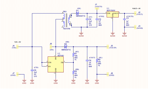
MCP1661 has been developed for applications that require higher output voltage capabilities. MCP1661 can regulate the output voltage up to 32V and deliver 125 mA typical load at 3.3V input and 12V output. At light loads, MCP1661 skips pulse to keep the output voltage in regulation, but the voltage ripple is maintained low. The regulated output voltage should be greater than the input voltage. The circuit diagram of the reference design is shown below:

This application uses MCP1661 as an open-loop flyback converter, the primary winding of the transformer being used as an inductor for the boost converter that clamps the primary output voltage (VOUTP) at around 13.5V. It is essential (for the normal operation of the entire circuitry and to avoid damaging some electronic components) not to connect any additional load between VOUTP and GND. The output voltage of the flyback converter (VOUTS) drops with the increase of output current since the feedback is taken from the primary side. To achieve a good output voltage regulation in the secondary side (VOUT), a 5V LDO is placed after the rectifying diode of the flyback converter, therefore the decrease of VOUTS when increasing the load is not critical. The MCP1661 Isolated Flyback Converter Reference Design can be used for USB-powered applications, where a positive, regulated 5V output voltage is needed from an isolated input voltage that varies from 4.75V to 5.25V.
Features of MCP1661 Flyback Converter Reference Design
• Input Voltage: 4.25V – 5.25V, Typical
– USB standard input voltage range
• Output Capability:
– Over 200 mA (at VOUT = 5V)
– Galvanic isolation
– Short-circuit protection
• Efficiency: up to 75%
• PWM Operation at 500 kHz
Microchip has tested this reference design. The company has also provided additional resources such as schematics, Gerber files, etc. You can find additional data about the reference design on the company’s website. To read more about this reference design click here.


