 Quiz-type game shows are increasingly becoming popular on television these days. In such games, fastest finger first indicators (FFFIs) are used to test the player’s reaction time. The player’s designated number is displayed with an audio alarm when the player presses his entry button.
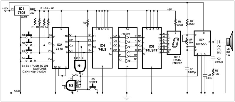
The circuit presented here determines as to which of the four contestants first pressed the button and locks out the remaining three entries. Simultaneously, an audio alarm and the correct decimal number display of the corresponding contestant are activated.
When a contestant presses his switch, the corresponding output of latch IC2 (7475) changes its logic state from 1 to 0. The combinational circuitry comprising dual 4-input NAND gates of IC3 (7420) locks out subsequent entries by producing the appropriate latch-disable signal.
Priority encoder IC4 (74147) encodes the active-low input condition into the corresponding binary coded decimal (BCD) number output. The outputs of IC4 after inversion by inverter gates inside hex inverter 74LS04 (IC5) are coupled to BCDto- 7-segment decoder/display driver IC6 (7447). The output of IC6 drives common anode 7-segment LED display (DIS.1, FND507 or LT542).
The audio alarm generator comprises clock oscillator IC7 (555), whose output drives a loudspeaker. The oscillator frequency can be varied with the help of preset VR1. Logic 0 state at one of the outputs of IC2 produces logic 1 input condition at pin 4 of IC7, there by enabling the audio oscillator.
IC7 needs +12V DC supply for sufficient alarm level. The remaining circuit operates on regulated +5V DC supply, which is obtained using IC1 (7805).
Once the organiser identifies the contestant who pressed the switch first, he disables the audio alarm and at the same time forces the digital display to ‘0’ by pressing reset push button S5.
With a slight modification, this circuit can accommodate more than four contestants.
More interesting projects available here.










I need a PCB layout of fastest finger first indicator without microcontroller
How many days it will take to deliver Manipal,karnaktaka
please ,explain it in clear and simple terms
PLEASE GIVE THE PURPOSE OF USING ICs-74LS,74LS47,7475,7805,NE555,4 INPUT NAND GATES CONCEPTUALLY
What is purpose of N1 and N2 nand gates
Hello sir, in the ic 74ls747 all the outputs are remaining high in all the cases on 5v.i replaced 3-4 ics and none are giving different output.please reply for the solution to this problem.
is the circuit cost effective?
Yes.