How best practices in circuit protection and board layout ensure long-term safety and reliability

From smart glasses to fitness-monitoring wristbands, wearable technology has become one of the hottest trends in the consumer electronics market, and these devices now permeate nearly every part of the average consumer’s daily life. According to Business Insider, the global wearables market is projected to grow at a compound annual rate of 35 percent over the next five years, reaching 148 million units shipped annually by 2019.
With the rapid growth of wearables, device manufacturers now have a greater vested interest in protecting both the technology and user. Due to their proximity to the skin, wearables are regularly exposed to static electricity generated by the user. If a device’s battery-changing interfaces, buttons, sensor circuits or data I/Os are left unprotected, electrostatic discharges (ESD) from human touch can damage those circuits and subsystems beyond repair. Designers must work to incorporate advanced circuit protection technologies to protect consumers who are increasingly dependent on wearables, as well as safeguard the products on which they are dependent.

As consumers demand improved wearable performance and smaller form factors, providing adequate circuit protection for these devices becomes more challenging. This article examines board layout strategies and circuit protection technologies that should be implemented early in the design process, as well as highlighting four steps for selecting ESD diodes that improve the safety and reliability of wearable designs.
Robust, Compact Circuit Protection
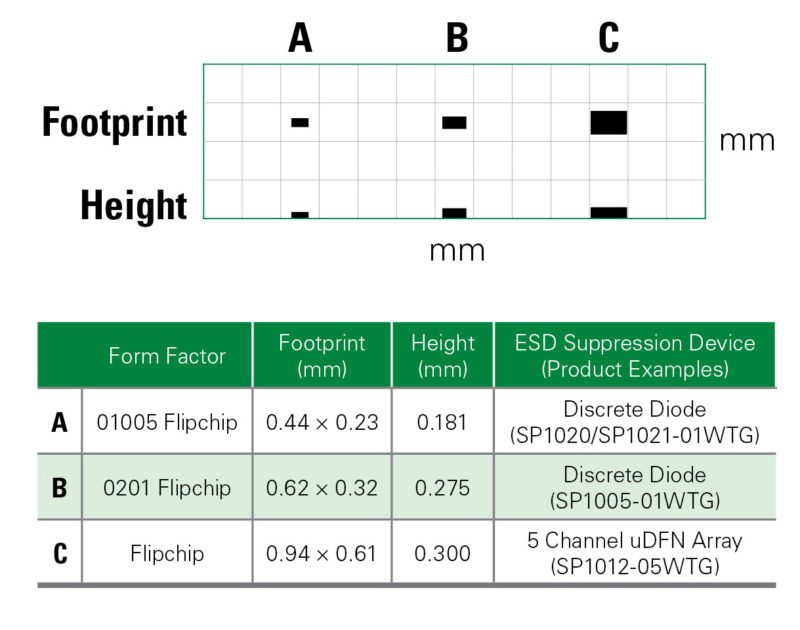
Steady improvements in back-end assemblies and wafer fabrication processes have made it possible to have robust ESD protection in a small form factor without degradation in ESD performance. For example, Littelfuse’s general purpose 01005 ESD diode has a dynamic resistance value of less than 1Ω and can withstand 30 kV contact discharge (IEC 61000-4-2). Despite its extraordinarily small dimensions (0.4mm x 0.2mm), the diode delivers the same level of ESD robustness and low clamping performance (dynamic resistance) as its larger counterparts (e.g., SOD882/SOD723 and 0201).

As the latest chipsets used in wearable devices get smaller and faster, circuit protection component form factors and performance must do the same.
Demanding operating conditions require robust circuit protection. The Human Body Model (HBM) test level of modern integrated circuits can reach 2,000 V, while most application designers ensure that their equipment meets at least Level 4 of the IEC 61000-4-2 test standard (15 kV air discharge, 8 kV contact). Many wearables and portable device manufacturer now have their contact discharge level raised to 15 or 20 kV, with some setting it as high as 30 kV — adding a new challenge. New designs in the ESD diode structures ensure that the compact ESD devices are robust enough to meet these demanding conditions for long-term operation and reliability.
Modern ESD protection manufacturing techniques can shrink the component’s board area usage. For example, a designer can save around 70 percent in board area by moving from the most common discrete form factor for ESD diodes, the SOD882 package (1.0 mm x 0.6 mm), to the 0201 form factor (0.6 mm x 0.3 mm). Furthermore, a designer can recognize a savings of over 85% when moving from the SOD882 to the 01005. It is essential to make these design decisions early in the process when flexibility in configuration and board layout is available.

The SP1012 Series Diode Array packs five ESD diodes in a flipchip package. Less than 1 square millimeter in size, these ESD diode arrays are helping circuit designers economize on both PCB space and costs.

Low-capacitance ESD diode arrays, like the SP3022 Series, are specifically designed for consumer electronics such as fitness bands, smart watches, smartphones and tablets..
Four-Step Guide to Selecting ESD Diodes
Design engineers can optimize the protection of their wearable designs by utilizing the following selection guidelines for ESD diodes:
1. Specify unidirectional or bidirectional: digital circuits and DC circuits traditionally use unidirectional ESD diodes, including pushbuttons and switches. AC circuits use bidirectional diodes, which may involve any signal with a negative voltage waveform greater than -0.7 V. AC circuits include legacy data ports, RF interfaces, analog video, and audio.
Unidirectional diode configuration performance improves during negative-voltage ESD strikes, so design engineers should opt to use these when possible. During these strikes, the clamping voltage will depend on the forward bias of the diode, which is typically less than 1.0 V. During a negative strike, bidirectional diodes provide a clamping voltage based on the reverse breakdown voltage, which is higher than the forward bias of the unidirectional diode. Therefore, by choosing the unidirectional configuration, engineers can dramatically reduce the stress on the system during negative strikes.
2. Decide location: Most wearable designs do not require board-level ESD diodes at each of the integrated circuits’ pins. The designer should determine which pins have exposure to the outside of the application where user-generated ESD events are likely to occur. If it can be touched by the user, the communication/control line is at risk to become a pathway for ESD to enter the integrated circuit. Typical circuits include button/switch control, audio, USB and other data buses; their pad layouts should be reduced to fit 0201 or 01005 outlines and optimize board space usage.
3. Review length of trace: Several considerations for trace routing should be made to safeguard the integrated circuits’ pins using a ESD diode—from I/O to ground. Unlike lightning transients, ESD does not unleash a large amount of current for a long duration. It is necessary to move the charge from the protected circuit to the ESD reference as quickly as possible to cope with ESD. The length of the trace—from the I/O line to the ESD component and from the ESD component to ground—are the overriding factors, not the width of the trace to ground. To limit parasitic inductance, the length of the trace should be kept as short as possible. This inductance will result in inductive overshoot—a brief voltage spike that can reach hundreds of volts if the stub trace is long enough. Recent package developments include µDFN outlines that fit directly over the data lanes to eliminate the need for stub traces.
4. Examine HBM, Machine Model (MM) and Charged Device Model (CDM) definitions: These test models are used by the semiconductor supplier to characterize the ESD robustness of the integrated circuits that run the portable or wearable device. Most suppliers have excellent in-house ESD policies and reduce the voltage test levels to save die space.
While these strict ESD policies benefit the supplier, the application designer ends up with a chip that is very sensitive to application-level ESD, which must not be allowed to fail due to field-level or user-induced ESD. To succeed, the designer must select a board-level device that is robust enough to protect against intensifying electrical stresses, but with low enough clamping to protect the sensitive integrated circuitry. It is important to consider IEC 61000-4-2 and dynamic resistance when evaluating an ESD protection device.
Conclusion
The rapid growth of the wearable market has made it ever more necessary for design engineers to consider circuit protection and proper board layout practices early in the design process to ensure long-term safety and reliability. ESD diodes are designed to work with small form factors and high levels of ESD robustness to safeguard wearable devices and their users. Key steps to provide ESD circuit protection for wearables include determining the TVS diode configuration, diode location, and length of the trace.
Additionally, decreases in HBM, CDM and MM test voltages are challenging designers to find protection solutions that account for ESD robustness (or lack thereof) of the wearable’s electronics to meet the protection needs of this highly sensitive circuitry. Lastly, at the same time the ESD protection is being considered, overcurrent protection of the charging line and battery should be attacked. Littelfuse has a full line of space efficient surface-mount fuses and Resettable PTCs to protect those circuits.
About the Author
Jim Colby is a manager of semiconductor business development at Littelfuse, Inc. His responsibilities include introducing new products to markets, as well as identifying and developing strategic growth markets. He received his BSEE from Southern Illinois University (Carbondale) and his MBA from Keller Graduate School of Management (Schaumburg). He has been with Littelfuse for over 15 years and has worked in the electronics industry for more than 23 years.