


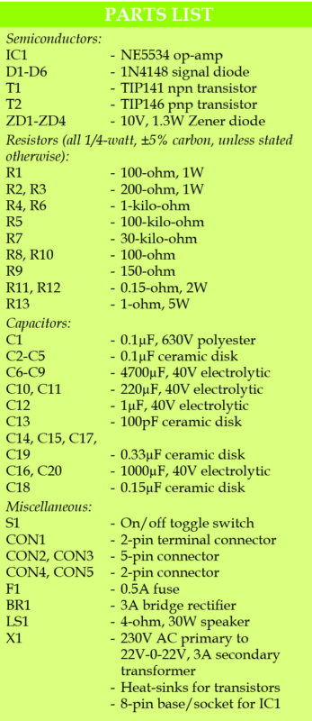
 There are many different audio power amplifier ICs to choose from, but designing an audio power amplifier using an operational amplifier (op-amp) and bipolar transistors is quite advantageous.
Compared to audio ICs, power transistors are easy to replace in case of damage and have relatively:
1. Very high power dissipation
2. Very high maximal working voltages and collector currents
3. High maximal working temperature

Here, we use an NE5534 operational amplifier and two Darlington transistors (TIP141 and TIP146) to produce a 30W audio amplifier.
NE5534 was selected because it has maximal working power supply up to ±22V, significant bandwidth, low total harmonic distortion (THD), high slew rate and output current more than ±20mA.

Circuit and working
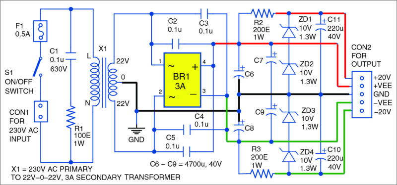
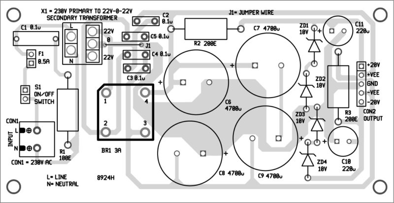
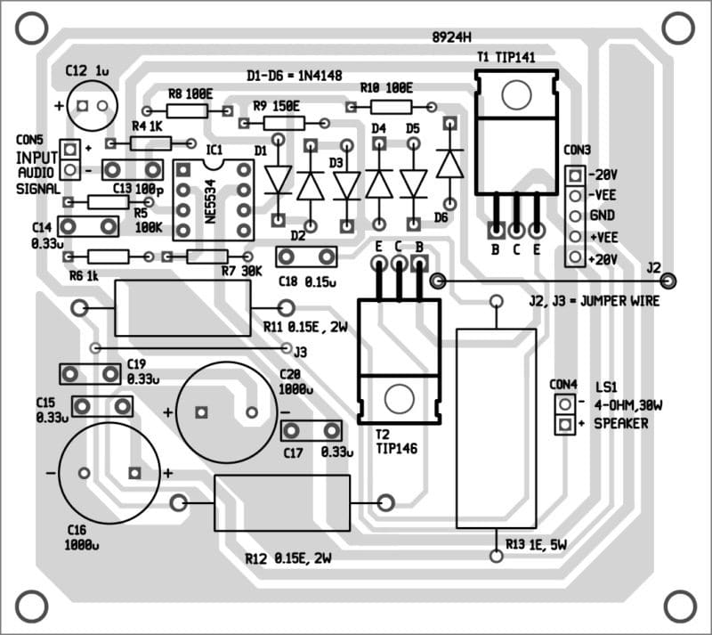
Fig. 1 shows the power supply section. Fig. 2 shows the circuit of the audio power amplifier using NE5534 and power transistors.
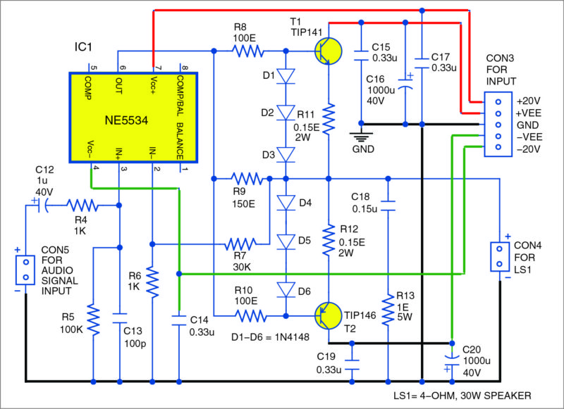
In the audio power amplifier circuit, the audio signal is applied to CON5. Capacitor C12 blocks the DC input signal. Resistor R4 and capacitor C13 limit the frequency of the input signal. Resistor R5 (100-kilo-ohm) determines the input resistance of the amplifier. The amplifier’s gain is determined by resistors R6 and R7 as follows:
Gain=1+R7/R6
=1+30k/1k=31
The amplifier’s gain can be set to any appropriate value above 3 because NE5534 is stable at gains higher than 3. Resistors R8 through R10 reduce the total harmonic distortion of the amplifier. Capacitor C18 and resistor R13 increase the amplifier’s stability and reduce THD. Darlington transistors T1 and T2 amplify the output current of NE5534.
Output current
The output current should be limited to around 4A. Diodes D1 through D3 and resistor R11 limit the output current of T1 (npn). Diodes D4 through D6 and resistor R12 limit the output current of T2 (pnp). Diodes D1 through D6 (each 1N400X or 1N4148) are mounted on the heat-sinks of transistors T1 and T2.
Here, R11=R12 =R=0.15-ohm to 0.22-ohm. The maximal output current is calculated as:
Imax=0.65V/R=0.65V/0.18-ohm
=3.6A or
Imax=0.65V/R=0.65V/0.15-ohm
=4.3A
Output power
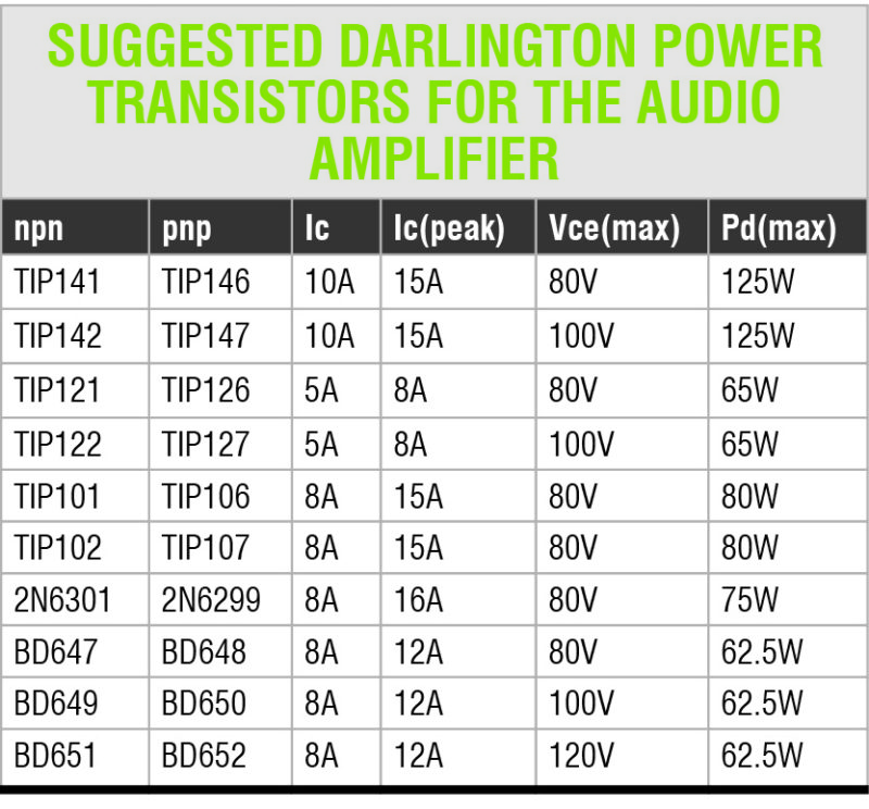
The output power of the amplifier depends on the power supply, power transistors, the size of heat-sinks and the load resistance. The heat-sink should have thermal resistance below 2oC/W and transistors should be isolated from the heat-sink. The amplifier outputs around 30W, which is enough to drive a 4-ohm load. Each of transistors T1 and T2 should have a gain of more than 800 at collector current of 4A.
The maximal power dissipation of each of the transistors should be preferably more than 40W and the peak output current more than 6A. Some of the suggested Darlington transistor pairs are listed in the table.
Power supply
The power supply circuit is shown in Fig. 1. It outputs four voltages: +20V, –20V, +VEE and –VEE. Transformer X1 is rated at 22V-0-22V, 3A. Bridge rectifier BR1 can be formed using 1N540X, CBR3A or BR305 diodes. Unregulated power supply (±VEE) is used only for the output Darlington transistors. It can go up to ±40V depending on the transistors. The regulated power supply is limited by resistors R2 and R3, and Zener diodes ZD1 through ZD4 to provide ±20V for op-amp NE5534. Though the maximal power supply for NE5534 is ±22V, it should not go beyond ±20V.
The circuit does not need any adjustment to work.
Construction and testing
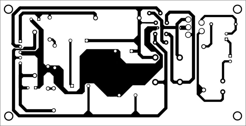
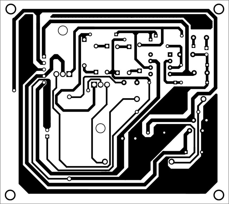
A PCB layout of the power supply circuit is shown in Fig. 3 and its components layout in Fig. 4. PCB layout of the 30W audio amplifier using NE5534 and Darlington transistors is shown in Fig. 5 and its components layout in Fig. 6.
Download PCB and component layout PDFs: click here
Assemble the circuits on their respective PCBs. Connect primary terminals (L and N) of the transformer to L (line) and N (neutral) marked on the power supply PCB at X1. Similarly, connect secondary terminals of X1 to 22V, 0, 22V marked on the PCB.
On the amplifier PCB, connect CON2 (from the power-supply PCB) to CON3 using suitable 5-core wires for power connections. Connect a 30W, 4-ohm speaker to CON4. At CON5, feed audio signal from any audio source like a mobile phone.
Now, connect 230V AC mains power supply to CON1. When you switch on the circuit through switch S1, you should be able to hear amplified sound from the speaker connected at CON4.

Hi, I found mistake in this circuit. output of the amplifier connected to diodes d3 and d4 is wrong in the circuit as well as in the PCB. please check.
Can you please elaborate why you think so? The use of these diodes have been explained under ‘Circuit and working’ section in the article above.
How can I do this for a 4ohm 40watt speaker
Here’s the reply received from the author Mr Petre Petrov :
You can connect 4 Ohm/40W speaker under the following restrictions:
ICmax < = 5.0 A,
Max power supply up to +/-25V
Appropriate heat-sinks for the transistors. e.g Rth <1.5C/W
Appropriate fast fuses, e.g. for 5A
Also you can use more powerful Darlington transistors.
22-0-22 v, 3A transformer is not readily available in market. Where to get it ?
Since I don’t have 30 watts speakers with me, what changes are needed in this circuit to get 10 and 20 watts respectively ?
Please suggest values of components needed for change if any.
If I want to use two numbers of this circuit for making stereo version, what should be voltage & ampere rating of transformer ?
Also, what should be size of heatsink (dimensions in length and width) which is not mentioned in any amplifier project here ?