This circuit has been developed to add a USB charging port to a bicycle for charging a mobile phone. The input supply for the circuit is produced by a dynamo (6V, 3W dynamo) in the bicycle. The circuit uses few components, which help in keeping the size, weight and cost of the unit down.
Circuit and working
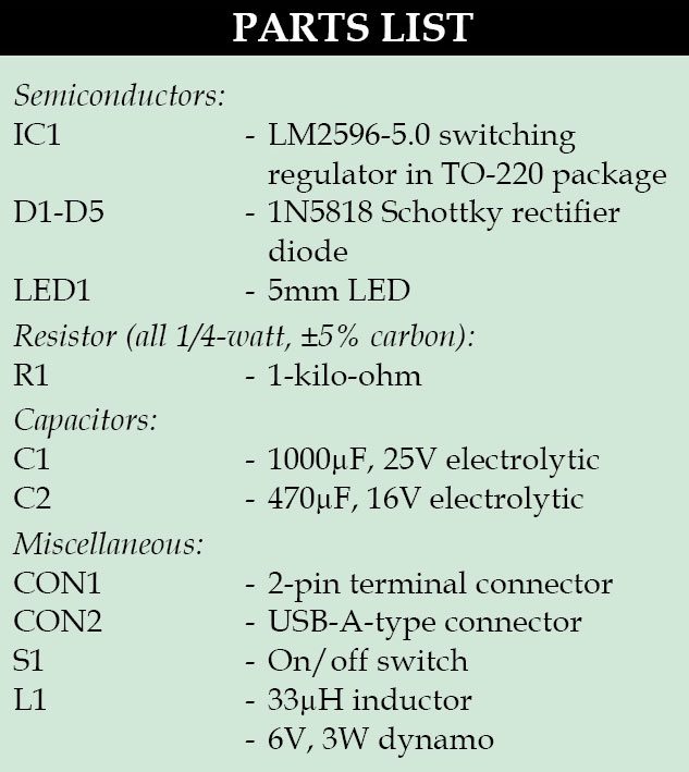
The circuit is based on LM2596-5.0 (IC1). Its configuration, with minor changes, generally reflects the recommendations included in Texas Instruments’ datasheet of LM2596-5.0. The IC provides all active functions for a step-down (buck) switching regulator, capable of driving a 3A load with excellent line and load regulation.
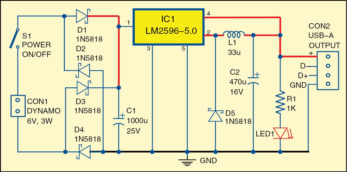
The output of the regulator is 5V. It operates at a switching frequency of 150kHz, thus allowing smaller-sized filter components than what would be needed with traditional lower-frequency switching regulators. Fig. 1 shows the circuit diagram of the bicycle USB charger.

 The alternating voltage generated by the dynamo is converted to DC by a full-wave bridge rectifier comprising Schottky barrier rectifier diodes D1 through D4 and a filtering electrolytic capacitor (C1). The output of the bridge rectifier, which is charged to peak value of AC voltage (nearly 10V), is input to switching regulator LM2596-5.0 to provide a regulated 5V (DC) output, which is suitable for charging mobile devices using the USB connector.
The 5mm LED (LED1) in the circuit indicates output status. Feedback connection FB (pin 4 on IC1) is connected directly to output voltage at electrolytic capacitor C2. As with all switching regulators, C2 should have a low ESR (equivalent series resistance) rating. Besides, 33μH inductor (L1) should be rated for a DC current of at least 1A. The dynamo output is connected to the circuit by switch S1.
Construction and testing
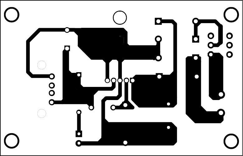
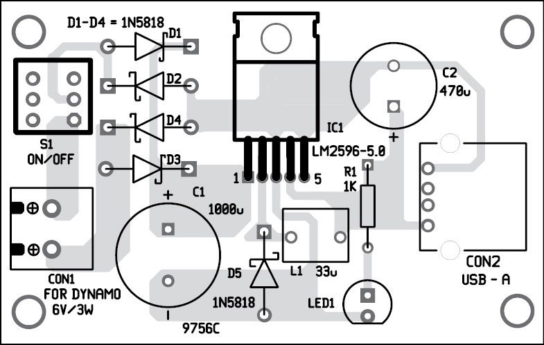
An actual-size, single-side PCB of the bicycle USB charger is shown in Fig. 2 and its component layout in Fig. 3. Assemble the circuit on the PCB in such a way that you can connect the mobile phone through a USB connector.


Download PCB and Component Layout PDFs: click here
LM2596 (IC1) is available in a standard TO-220 package as well as in a surface mount TO-263 package. The PCB layout is for TO-220 package. The whole circuit can be easily constructed even on a perforated prototyping board. The USB output is soldered directly in the prototyping board. However, it is very important to observe correct polarity when connecting the USB output socket. After construction and testing, enclose the unit in a suitable ABS/acrylic box.
T.K. Hareendran is an electronics hobbyist, freelance technical writer and circuit designer


