


 Over-voltage protection circuits are used to protect voltage-sensitive loads. Voltage transients may occur due to a number of reasons such as transformer switching, load switching, and short/open circuit in rectifier and regulator circuit. Such transients can affect proper functioning of an electronic circuit or even damage it. Hence it is necessary to use an over-voltage protection circuit to protect expensive loads against all the sources of voltage transients.
In electronics engineering, where over-voltage protection experiment is included in the syllabus, the present circuit can be used to very effectively demonstrate the effect to students.

Circuit and working
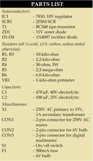
Fig. 1 shows the demo circuit for over-voltage protection. It is built around a rectifier comprising four 1N4007 diodes (D1 through D4), 10V voltage regulator IC 7810 (IC1), SCR 2P4M (SCR1), transistor BC548 (T1) and a few other components. SCR1 is used as a protective component.
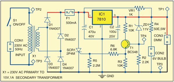
If voltage exceeds beyond the withstanding voltage capacity of the device that needs to be protected (6V bulb here), the circuit disconnects the device from supply. To demonstrate this, potmeter VR1 connected across regulator IC1 is used to increase the voltage at the output of regulator IC1. When the output voltage of IC1 increases, voltage at the base of transistor T1 also increases, which triggers SCR1 through resistor R6. Once SCR1 triggers, fuse blows and disconnects the power supply from the device.

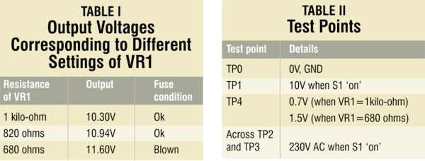
For demo, set VR1 at the maximum limit (say, 1k) and switch on the circuit. Using a digital multimeter, measure the output at CON3. It should be around 10.3 V. Now reduce VR1 resistance in steps. At around 800 Ω, the multimeter reads 10.9 V. Reduce the resistance further until SCR1 fires. Experimentally, it was found that at around 680 Ω, the SCR turns on after receiving a triggering pulse and a heavy current passes through the fuse wire. Due to this, the fuse wire blows and the load disconnects from the supply.
Construction and testing
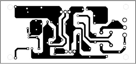
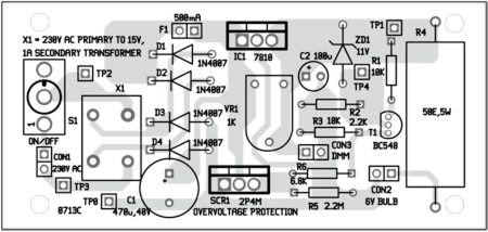
A single-side PCB of the demo circuit for over-voltage protection is shown in Fig. 2 and its component layout in Fig. 3. After assembling the circuit on PCB, enclose it in a suitable box.
Download PCB and component layout PDFs: click here
To test the circuit for proper functioning, switch on S1 and measure the input voltage (230V AC) between TP2 and TP3. Also verify the output of IC1 as 10 V at TP1 with respect to TP0. Check voltage variation at the base of transistor T1 corresponding to change in the resistance value of VR1.
Milind M. Sutar is an assistant professor and Dr J.L. Bhosale is an associate professor at the Department of Physics at Shikshan Maharshi Dr Bapuji Salunkhe Collge, Miraj. Prof. P.B. Joshi is a professor and director at School of Physical Sciences, Department of Physics, Solapur University, Solapur
