In continuation of the embedded control applications explained in Part 2, let’s now examine the use of inbuilt functions of AVR ATmega8535 (such as output compare, ADC and UART) for various applications.
PWM operation of ATmega8535
When the AVR is configured for pulse-width modulated (PWM) operation, the PWM outputs become available at output-compare pins 18 (OC1A) and 19 (OC1B) of ATmega8535. PWM, in conjunction with an analogue filter, can be used to generate analogue output signals and thus it serves as a digital-to-analogue converter.
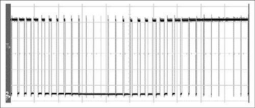
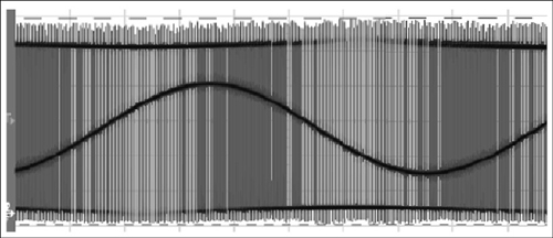
Principle of pulse-width modulation. To generate different analogue levels, the duty cycle and thereby the pulse-width of the digital signal (base frequency) is changed. If a high analogue level is needed, the pulse width is increased and vice versa (see Figs 15 and 16).
A digital pulse train with a constant period (fixed base frequency) is used as the basis. The base frequency, which can be programmed suitably, should be much higher than the frequency of the output analogue signal obtained after filtering out the base frequency component. For example, to generate a sinewave signal of low frequency (say, 10 Hz, as used for drives or controls), the base frequency of rectangular pulses (with varying duty cycle) may be of the order of 1 kHz or more.
Pulse generation method. The scheme for pulse generation is as follows: Timer/counter 1 is used to count clock ticks. If 8-bit PWM is selected, after the timer counts up to ‘255,’ its count is decremented with each clock tick. Thus, the number increases up to ‘255’ and then decreases, resembling a triangular pattern.
When the number stored in the output-compare register (OCR) matches the loaded count value, pin 19 (output-compare action pin) becomes high or low, as programmed. For example, if the OCR is loaded with a value of ‘l00,’ the logic state of OCR pin will be:
Count value OCR pin
0 to 100 Low logic
100 to 255 High logic
255 to 100 High logic
100 to 0 Low logic
Thus, for the total time taken to count 255×2=510 clock ticks, the output pin (pin 19) will be high for (2×155)/(2×256) or 60.5 per cent of the total triangular wave time of one PWM pulse (or the PWM pulse will have a duty cycle of 60.5 per cent). Thus, effectively the voltage transmitted in this period is 60.5 per cent of the maximum, because the pulse is high only for this period of time.
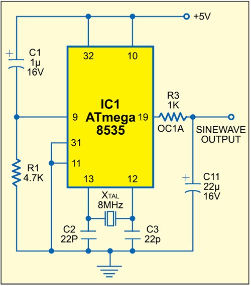


The following program (avrsine.asm) will generate a 1Hz sine wave (after filtering) on pin 19 using PWM:
[stextbox id=”grey”]
AVRSINE.ASM
;———————————————————————
; File: avrsine.asm
; Description: Example of how to use the fast PWM
; of the Avr to generate “sine-wave” signal. The PWM
; output requires filtering to shape the sine wave
; form.
;———————————————————————
.include “m8535def.inc”
rjmp init
;Interrupt vector table
.org OVF1Addr ;OC1Aaddr
; Interrupt vector for timer1 output compare match A
rjmp TOF_isr
;Main code
init:
ldi R16,low(RAMEND)
; Load low byte address of end
of RAM into register R16
out SPL,R16
; Initialize stack pointer to end of internal RAM
ldi R16,high(RAMEND)
; Load high byte address of end of RAM into
register R16
out SPH, R16
; Initialize high byte of stack pointer to end of
internal RAM
ldi r16,$ff
out ddrb,r16
ldi r16,$55
out portb,r16
ldi r16, (1<
out DDRd, r16 ;since that is the PWM
output pin 19
;SELECT CLOCK SOURCE VIA TCCR1B
LDI R16,$81
;8 BIT PWM NON-INV.
; Set PWM mode: toggle OC1A on compare
out TCCR1A, r16
; Enable PWM
ldi r16, 0xFF
; Set PWM top value: OCR1C = 0xFF
out OCR1AL, r16
LDI R16,0
OUT OCR1AH, R16
; Enable Timer/Set PWM clock prescaler
LDI R16,02
OUT TCCR1B,R16 ;ck/8 as pwm clock
(1MHz/8 = 125 kHz)
ldi r16, (1<
Ovrflow interrupt
out TIMSK, r16
clr r17
clr r18
sei
; Enable global interrupts
idle:
ldi r16, (1<
out MCUCR, r16
sleep
rjmp idle
TOF_isr:
ldi ZH, high(sine_table*2)
; Set up Z to point to the beginning of
sine_table
ldi ZL, low(sine_table*2)
add ZL, r17
; Offset Z by r18:r17
adc ZH, r18
lpm
; Load sine_table[Z] into OCR1A
out OCR1AL, r0
inc r17
reti
sine_table: ; 256 values
.db 128,131,134,137,140,144,147,150,153,156,159,162,
165,168,171,174
.db 177,179,182,185,188,191,193,196,199,201,204,206,
209,211,213,216
.db 218,220,222,224,226,228,230,232,234,235,237,239,
240,241,243,244
.db 245,246,248,249,250,250,251,252,253,253,254,254,
254,254,254,254
.db 254,254,254,254,254,254,254,253,253,252,251,250,
250,249,248,246
.db 245,244,243,241,240,239,237,235,234,232,230,228,
226,224,222,220
.db 218,216,213,211,209,206,204,201,199,196,193,191,
188,185,182,179
.db 177,174,171,168,165,162,159,156,153,150,147,144,
140,137,134,131
.db 128,125,122,119,116,112,109,106,103,100,97,94,91,
88,85,82
.db 79,77,74,71,68,65,63,60,57,55,52,50,47,45,43,40
.db 38,36,34,32,30,28,26,24,22,21,19,17,16,15,13,12
.db 11,10,8,7,6,6,5,4,3,3,2,2,2,1,1,1
.db 1,1,1,1,2,2,2,3,3,4,5,6,6,7,8,10
.db 11,12,13,15,16,17,19,21,22,24,26,28,30,32,34,36
.db 38,40,43,45,47,50,52,55,57,60,63,65,68,71,74,77
.db 79,82,85,88,91,94,97,100,103,106,109,112,116,119,
122,125
[/stextbox]
For observation of the sine wave on an oscilloscope, use a low-pass filter comprising a 1-kilo-ohm resistor (series element) and a 1µF capacitor (shunt element). However, with an analogue multimeter, the sine wave can be directly observed at pin 19.
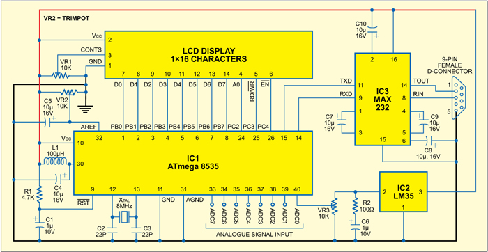
In the avrsine.asm program, for each of the triangle wave periods, we read a table of sine values (multiplied by ‘256’) and load these values one by one into the OCR. Since the values vary in a sinusoidal pattern, the pulses that come out are also pulse-width modulated as per these values (see the oscilloscope pattern shown in Fig. 16).
To do the table look-up (as given in the example program ‘LCD Table.ASM’ of Part 1), the LPM instruction is used. The Z register is used as an indirect indexed register. As stated earlier, the LPM instruction fetches from the table one byte into r0. The actual loading of the OCR value is done by the instruction:
[stextbox id=”grey”]out OCR1AL, r0[/stextbox]
where OCR1AL refers to pin 19. (OCR1BL refers to pin 18, which is not used here.)


