 Circuits like Geiger counters, insect zappers, Nixie tubes and sensors require high-voltage direct-current (HVDC) supplies. There are various types of HVDC power supply designs available in the market, including voltage doubler or quadrupler, flyback converter and boost converter.
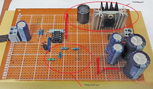
Some of these have low current-output capacity. But with right calculations using basic boost conversion formulae, we may achieve HVDC supplies capable of clean and high current capacity. Application notes supplied by component manufacturers provide many handy formulae compatible with their components that are derived from these basic formulae. Presented here is a boost converter design using MC34063 DC-DC converter. The author’s prototype is shown in Fig. 1.
Boost converter basics
In a boost converter (Fig. 2), energy is stored in the inductor (L1a) during the time the transistor (T1a) is ‘on’ (ton). When the transistor is turned off (toff), the energy is transferred in series with input Vin to the output filter capacitor (Cout) and load (RL). This configuration allows setting of the output voltage to any value greater than the input.
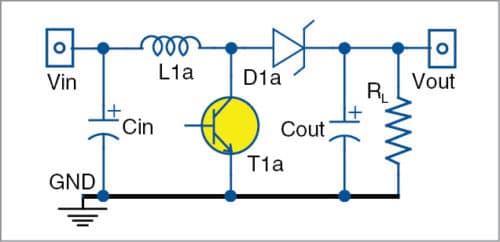
The output voltage can be calculated as follows:
Vout=Vin(ton/toff)+Vin, or
Vout=Vin((ton/toff)+1)
Circuit and working
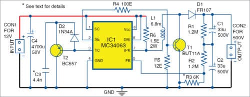
Circuit diagram of the boost converter using MC34063 DC-DC converter is shown in Fig. 3.
MC34063 is a monolithic control circuit containing all the active functions required for switching DC-to-DC converters. It represents significant advancements in ease of use with highly efficient, yet simple switching regulators. The use of switching regulator is becoming more pronounced than linear regulators because of the size and power-efficiency requirements of new equipment designs. Switching regulators increase application flexibility while reducing the cost.
MC34063 was designed for buck, boost and voltage-inverter converter applications. It includes temperature-compensated reference voltage, oscillator, active peak-current limit, output switch and output-voltage-sense comparator. All these functions are contained in an 8-pin DIP or SOIC package.
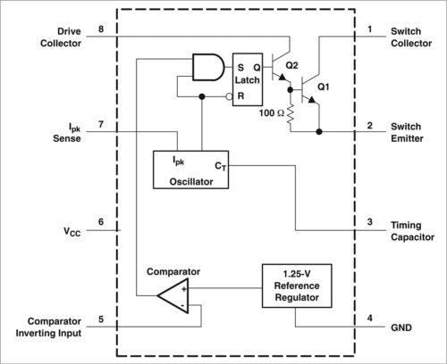
Internal diagram of MC34063 as per the datasheet given by Texas Instruments is shown in Fig. 4.
Its pin 5 (comparator inverting input) senses and sets the output voltage to a stable value for calculating feedback resistor values as shown in Fig. 5.
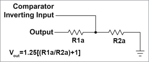
Vout=1.25((R2a/R1a)+1)
The internal voltage regulator produces 1.25 volts for the internal comparator, so the external voltage divider comprising R1a and R2a should be arranged such that it gives exactly 1.25 volts when the desired output voltage is reached. For example, if you need output voltage of around 501 volts, the voltage-divider resistor values must be R2a=2.4 mega-ohms and R1a=6 kilo-ohms, respectively.
As shown in the block diagram, the comparator output triggers and disables the SR latch. The oscillator driven by the timing capacitor at pin 3 is composed of a current source and sink elements, which charge and discharge the external timing capacitor between upper and lower preset thresholds. Typically, charge and discharge currents are 35mA and 200mA, respectively, yielding approximately a 6:1 ratio. Thus, the ramp-up period is six times longer than the ramp-down period. The upper threshold is equal to internal reference voltage of 1.25V, and the lower threshold is approximately 0.75 V.
The oscillator runs continuously at a rate controlled by the timing capacitor value. It also senses peak current by sensing the voltage generated by the inductor current across a small-value, higher-wattage sensing resistor connected to pin 7. In this circuit (Fig. 3), 1.5-ohm, 2W resistor R6 is the sensing resistor.
As shown in the block diagram, the output switch is an npn Darlington transistor. The collector is tied to pin 1, and the emitter is tied to pin 2. This allows the designer to use MC34063 in buck, boost or inverter configurations. The maximum collector-emitter saturation voltage at 1.5A (peak) is 1.3V, and the maximum peak current of the output switch is 1.5A. For higher peak output current, an external transistor can be used. The oscillating pulses drive the internal transistors, which may be used to provide boost/buck conversion or to drive an external power transistor of higher rating to get higher power rating.
Some circuit designs, mainly step-up and voltage-inverting, require ton/(ton+toff) ratio greater than 0.857. This can be obtained by adding a ratio extender circuit, which uses germanium diode and is temperature-sensitive. A negative-temperature-coefficient timing capacitor will help reduce this sensitivity. In Fig. 3, the extender circuit consists of transistor T2 (BC557), germanium diode D2 (1N34A) and timing capacitor C3. Here, T2 is not driving anything but a discharging and charging switch for capacitor C3 powered by pin 3 of the IC. Current limiting must be used on all step-up and voltage-inverting designs using the ratio extender circuit. This allows the inductor time to reset between cycles of over-current during initial power-up of the switcher. When the output filter capacitor reaches its nominal voltage, the voltage feedback loop controls regulation.
In the main circuit, a wire is connected between the junction of resistors R1 and R2 and capacitors C1 and C2 for charge balancing in both output capacitors. Only resistor R3 connected to pin 5 of MC34063 forms the voltage divider.
Software
We have designed a utility software to find out component values quicker for rapid prototyping of a power supply based on MC34063. The software program is written using HTML and JavaScript, and can be incorporated in a system having PHP installed. It runs under PHP development environment. HTML is a front-end software, whereas PHP is a back-end software. JavaScript file checks for blank fields in HTML form. PHP is incorporated in a web server. So multiple user clients within a network, such as in a lab or college, can use this software simultaneously. The program is developed using NetBeans IDE for PHP.
Download source code
Software installation.
1. Download WampServer (for localhost development) from www. wampserver.com/en/ and NetBeans IDE from https://netbeans.org/features/php/. Install these in your Windows PC. Install appropriate Visual C++ extension (here VC++ 2012) before installing WampServer to get all prerequisite dll files for smooth running of the IDE and Apache server environment.
2. WampServer runs in the background with the option in online mode. Make sure WampServer icon on the taskbar turns green.
3. Create a folder, say, HighVoltage, under C:\wamp\www folder. Copy HVBoostCalculator.html, HVDesign.js and HVcircuit.jpg image files into the project folder.
4. Create a new PHP project in NetBeans. Select ‘PHP Application’ option and click ‘Next.’ A project folder will create automatically. Note that your HighVoltage folder is under this project folder.
5. Under ‘Run Configuration’ window, select ‘local server’ option in Run As: field. Then, click ‘OK’ to proceed.
HVBoostCalculator.html is HTML script and its associated image is HVcircuit.jpg.
HVDesign.js is Javascript script. Run the HVBoost Calculator.html to get the page as shown in Fig. 6.
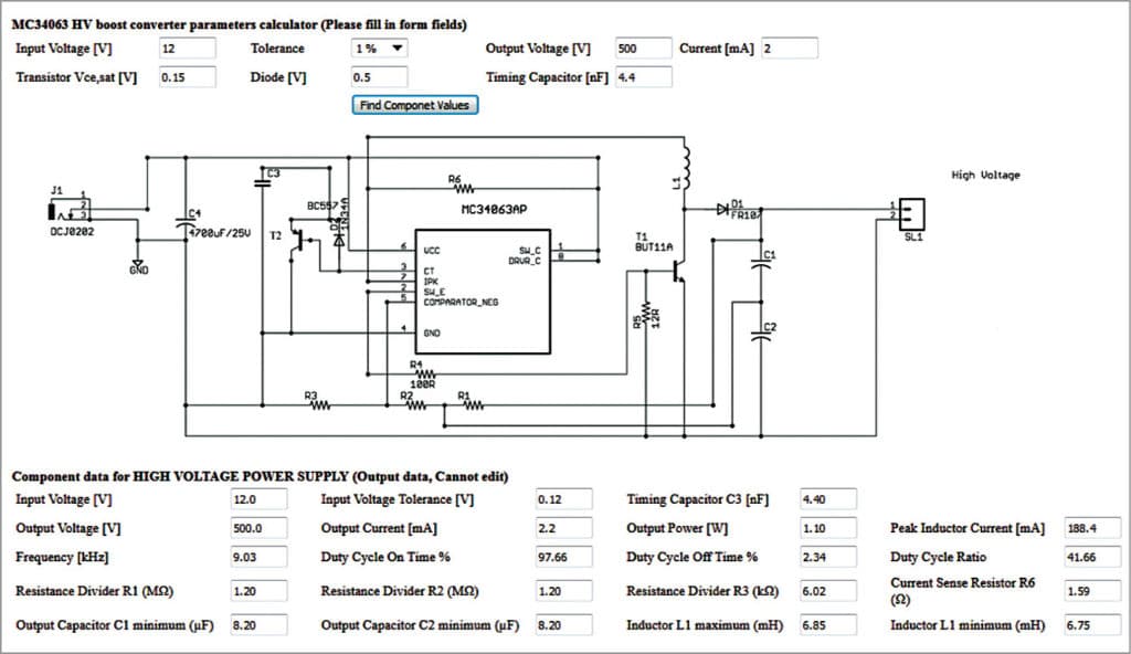
First, you need to feed 9-12V DC input and voltage tolerance depending on the supply you are using; generally, voltage tolerance is 1 per cent. Then specify the required output voltage and current in the respective form fields. (For higher output voltages, please use transistor T1 with higher voltage and current specifications.)
Using the datasheet of power transistor T1, find its Vce saturation value and put in the form field. Also get forward voltage drop of diode D1 from its datasheet feed in the form field. These parameters are very crucial for calculation of component values. After all values have been filled up in the respective fields, click ‘Find Component Values’ button. The form is verified for blank fields and calculation is done for the components. You will get values of R1 though R3, R6, L1, C1 and C2 as well as circuit parameters like duty cycle, switching frequency and output power.
As shown in the program output screenshot, design the circuit for 12V input voltage DC, 500V DC output, 2mA output current and 4.4nF timing capacitor. From the program output, you get values of output capacitor as 8.20µF, sensing resistor R6 as 1.59 ohms (the nearest value of 1.50 ohms) and inductor L1 as 6.8mH. The complete circuit diagram of this design is shown in Fig. 3.
Construction and testing
An actual-size PCB layout of the HVDC power supply using MC34063 is shown in Fig. 7 and its components layout in Fig. 8. Use suitable heat-sink for transistor T1. Keep inductor L1 and transistor T1 away from the main circuit section. Preferably use a shielded-type inductor for L1.


Download PCB and component layout: click here
R6 should be 2W, flameproof resistor. Use the nearest value given by the software. Use proper heat-sink for power transistor T1. Keep inductor L1, transistor T1 and MC34063 away from each other on the board to minimise EMI interference.
For exact value of R3, use a parallel combination of resistors. For example, use a 6.8-kilo-ohm resistor in parallel with a 56-kilo-ohm resistor to get 6 kilo-ohms. Avoid using a trimpot because of thermal drift. Use capacitor C3 such that the frequency is within 10kHz, to avoid switching problems and heating of transistor T1.
Caution
Handle the high-voltage DC circuit with utmost care as it may cause electric shock.


This is very nice project. I want to buy this project materials in all respect, details of hardware related items, related shops in Mumbai- India. So can you help to provide it. Thanks lot.
BUT11A, MC34063 maybe available in Lamington road, I bought from there. Rest are general use components and be careful while selecting 450V capacitors
Wow, it looks useful! Thanks for your sharing.
मराठीत दिल्याबद्धल आभारी.
Thank you for your feedback.