


This short article describes a simple circuit capable to convert a TTL/CMOS PMW signal to an analog signal. The circuit can be used as an extension shield for Arduino with a simple MCU or with TTL/CMOS signal generator. It is useful to produce audio signals and signals for control DC motors, LEDs, incandescent lamps, and other peripheral devices.
Introduction
PWM based DACs are often used to produce analog signals from digital outputs. Usually the technical solutions for these PWM based DACs includes three main blocks:
- Digital PWM generator. Most frequently this is a MCU but we could use also a square wave generator (SQWG) or computing platform as Arduino.
- Analog integrator. In the simplest cases that is a single RC network. Sometimes the signal is for driving an electrical motor. In that case the role of the integrator can be executed by the RLC parameters of the motor.
- Analog output buffer or amplifier providing the necessary output voltage, current and power.
The main advantages of the PWM DACs are:

- Simplicity and low cost.
- High and digitally controlled resolution. The resolution can be 10 bits or even more because depends mainly on a digital counter.
- Possibility to obtain high output current, voltage and power.
Description of the proposed circuit
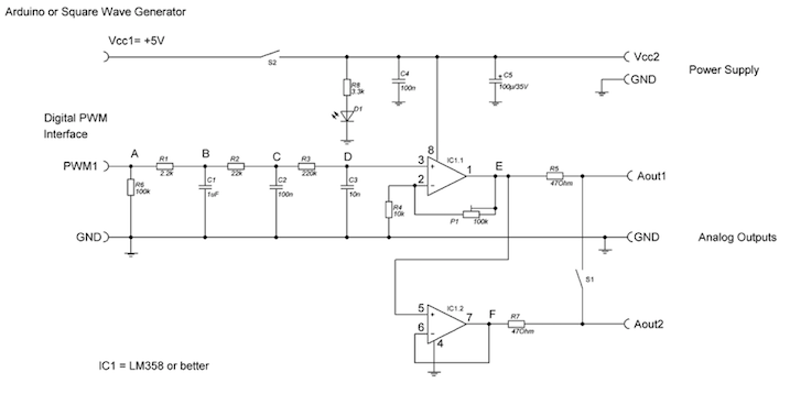
Figure 1 presents the circuit diagram of the low cost PWM module with two outputs.
The circuit consists of two parts:
- input passive RC low pass filters with three stages
- output stage with two operational amplifiers
The input passive low pass filter with three stages is build around R1, C1, R2, C2, R3 and C3.

The three cut-off frequencies of the three stages are calculated according to the formulas below.
For the first stage:
F(-3db)1 = 1/(6.28*R1*C1)
For the second stage:
F(-3db)2 = 1/(6.28*R2*C2)
For the third stage:
F(-3db)3 = 1/(6.28*R3*C3)
In most of the cases we should have:
F(-3db)1 = F(-3db)2 = F(-3db)3
R3 = 10*R2=100*R1
R1>=510Ohm
Here we have
F(-3db)1 = F(-3db)2 = F(-3db)3 = 72Hz
We may select any appropriate cut off frequencies for the RC filters. Here we will use the power supply of the computer as voltage reference source for the PWM.
The output stage is build around two OAs IC1.1 and IC1.2. Preferably we should use rail to rail OAs. We may use also the dual OA LM358 but the input and the output will be limited to around 3.5V.
If we close the switch S1 both OAs will work in parallel over the same load. If we open the switch S1 both OAs will produce the same voltage over separated loads. Preferably the loads should be above 2kOhm.
If we close the switch S2 we can use the power supply of the computer Vcc1, e.g. Arduino. If we open the switch S2 we can use other power supply Vcc2, e.g. up to 32V with LM358.
IC1.1 works as non inverting amplifier with gain defined by P1 and R4.
The minimal gain is Av1min = +1.
The maximal gain is Av1min = +11.
The gain is set according to the needs by P1, the required output voltage and the power supply of IC1. The gain is calculated with the simplified formula below:
Av1 = 1 + P1/R4
IC1.2 works as follower with gain Av2=+1.
Testing the expansion module
Figure 2 presets block diagram of the testing the module with computer or with digital signal generator and with digital voltmeter and oscilloscope.
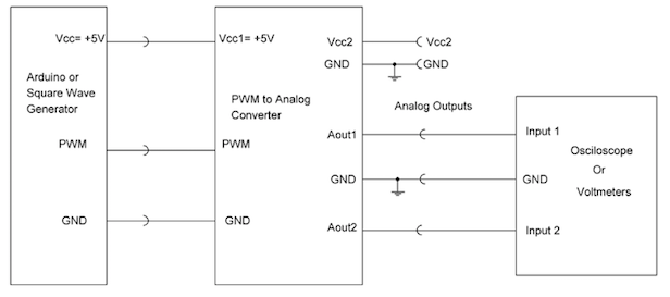
Please note that the maximal output voltage Aout1 and Aout2 depend on:
- The power supply of the OAs
- The position of the trimmer potentiometer P1
- The output voltage levels of the TTL/CMOS output driving the module
We should Fix the frequency of the PWN (e.g. 1000Hz) and we should change Thigh and Tlow of the pulses and we should test the output voltages. We can use the Table 1 in order to test the output voltages.
Table 1
Examples of reference voltages for testing the PWM board
| SQW signal Thigh/T, [%] |
approx. Vout as percentage of Voutmax | Example of Vout if we have Voutmax = 5.000V | Example of Vout if we have Voutmax = 3.000V |
| 0 | 0 | 0.0V = Vout min | 0.0V = Vout min |
| 10 | 10 | 0.5V | 0.3V |
| 20 | 20 | 1V | 0.6V |
| 30 | 30 | 1.5V | 0.9V |
| 40 | 40 | 2.0V | 1.2V |
| 50 | 50 | 2.5V | 1.5V |
| 60 | 60 | 3.0V | 1.8V |
| 70 | 70 | 3.5V | 2.1V |
| 80 | 80 | 4.0V | 2.4V |
| 90 | 90 | 4.5V | 2.7V |
| 100 | 100 | 5.0V = Voutmax | 3.0V = Voutmax |
Note: The linearity of the conversion depends to some degree from the parameters of the digital output.
Conclusions
That short paper presents simple and low cost solution of PWM to analog converters which can be used with Arduino or other digital computer. In most of the cases the produced analog signals are with relatively low frequency and consequently with relatively low slew rate. The OAs buffering the outputs of the PWM converters can be any appropriate OAs providing enough voltage, current and power at the output.
Caution should be made when the PWM duty cycle is too low or too high. The dangerous limits are set by every particular case.
Usually PWM <5% and PWM>95% are to be avoided in many cases due to possible complications with the following electronics and mechanical parts.
Using the analog signals produced with PWM as analog voltage reference should be avoided due to the ripples and instability and inaccuracy. In most of the cases the PWM DACs are good for diving LEDs, incandescent lamps, LCD displays, DC motors and sometimes loudspeakers. The spectrum of the rectangular signal produced by the PWM is large and variable and that can be a problem without appropriate filtering, construction and PCB layout.
Resistors, capacitors and operational amplifier for the filtering and buffering of the PWM signals should be with appropriate characteristics.
The term “accuracy” should not be mixed with the term “resolution”. Both terms are different.
Usually with the PWM DACs we may obtain high resolution but not very good accuracy.
These DAC are simple but can be misleading.
Attention can be paid to the PWM switch, the power supply and the analog components converting the digital signal into an analog signal.
References: Datasheets of the components in the circuit should be used.
