As we moved towards touchscreen phones with ultra-smart features, we also reduced the lifetime of our mobile phones. A case that comes to mind from personal experience is a phone bought in 2004 that was still functioning in 2014, and was decommissioned only when a different phone was bought.
The newer phones, however, do not look as if these are built to last. You eventually have to go for a change of device every couple of years or so. What does this say about the reliability of these devices?
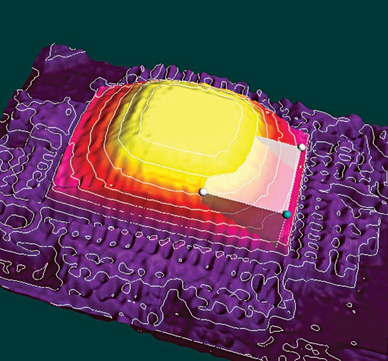
Major threat to the reliability of a printed circuit board (PCB) in an electronic device comes from the heat produced and improper dissipation of heat. Most aspects of the PCB such as traces, solder masks, white-marking, laminates and plating are relatively reliable and rarely fail in use. However, copper barrels in the vias and holes can lead to long-term operational failures. Hence, reliability begins with the designing of the PCB itself.

EDA tools help with the design
The new generation of electronic design automation (EDA) tools have been a huge help with PCBs. Satyan Prakash Raj, development engineer, Toradex, says, “Latest EDA tools support both pre- and post-layout simulations, and help engineers analyse and fix issues during the design stage, much before getting assembled, and test it.”
New EDA tools provide advanced routing features, design simulations including signal-integrity and post-layout automated design checks, PCB stack-up management and impedance calculations, which enable designers to build better circuit boards, lower design risks and bill of materials (BOM) management, among others.

Thermal management is a focus area in design.
Problems brought in by heat can be sorted out by effectively mitigating the heat by proper selection of material sets chosen for building the PCB. This includes the chemicals involved in the process. Multilayered board lamination, circuit density and plated through-hole (PTH) technology are also factors to be considered while building the boards. And the most important of all, take time to get the design right. You never know when the next Samsung Galaxy Note 7 will happen.
Raj adds, “Latest tools come with integrated simulation and analysis tools for thermal analysis and impedance calculation.” This could help in managing the problems caused due to heat generation at a later stage of the PCB build.
From a mechanical point of view, EDA tools allow you to generate and view the circuit board as a three-dimensional (3D) model. This would help you collaborate with mechanical designers. With support of rigid-flex design capabilities in the latest EDA tools, you can visualise the design in 3D and help check for mechanical issues like component collisions and clearance issues.
Open libraries are kind of a sour area.
Some EDA tools also offer integrated open source libraries to help pick available components to start with the design. Some online tools provide availability and pricing across vendors. However, Hrishikesh Kamat, chief executive officer, Shalaka Technologies, feels that, to get the best in design, you need to manually build the components instead of blindly trusting open source libraries. He adds, “We have our own library to go to in case of non-regular components.”
Anuj Deshpande, founder, Makerville Solutions, also believes in designing the components manually. He says, “A lot of times this can increase the timeline of the project, but the output is very reliable.” However, the saving grace for open libraries, as Deshpande explains, is the extensive use of standard components that are easily available in open libraries.
Kamat explains some designing issues his team faces, “We have to take care while defining the power and ground planes, and avoid auto-correct most of the times.” Auto-correct, on one hand, helps in getting the design right but, on the other, can cause unexpected problems while manufacturing.
Problems in manufacturing
When talking about manufacturing printed boards, the magic happens due to very minute particles. Dana P. Ilmer, Superior Flux & Manufacturing Co., says, “You have to be very careful with the manufacturing process. The smallest of problems can lead to very disastrous PCBs.” The boards need to be cleaned thoroughly and must be checked and rechecked for any remaining particles post processing before you add any components. He explains, “You cannot leave any flux on your boards post cleaning. Unless the board is clean of every individual particle, you are going to have problems.”
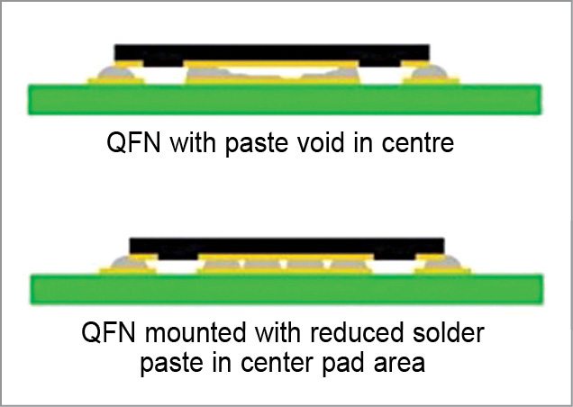
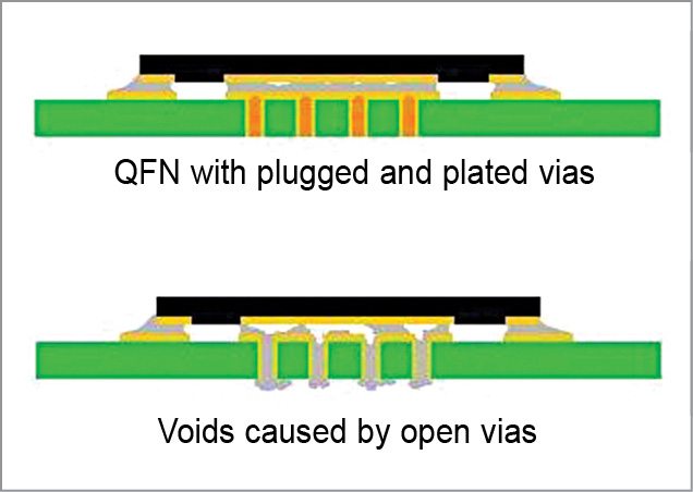
Through-hole is an area that sees a lot of problems. However, are there solutions that can take care of these. Improved plating distribution has had positive effects like improving the reliability of the PTHs. Electrolytic plating is a cost-effective method for doing this. It uniformly increases the thickness of circuits and results in improved tracks.For improved thermal shock and cycling, however, acid copper plating process is the one to go for. Throwing power can also be increased by improvements in plating cell design with anode configurations and proper selection of circuit components. Pulse plating could also help in this regard. Ilmer says, “There was once a case of phenolic paper boards being used for PCBs.”
The material for the board is also important.
Phenolic paper boards help in cutting cost, but bring in their own set of problems. Compared to glass epoxy boards, these have less adhesion for copper cladding and are more prone to environmental degradation and chemical attacks.
These are also mechanically weaker, which facilitates easy drilling and shaping. However, this ease can be easily looked over as these happen to be more brittle than glass epoxy boards. This highlights the fact that the material used in the boards is also a matter of concern.
Laminate materials present their own set of problems. These can be brittle and cause problems during inner layer treatment, leading to reduced bond strength between multiple layers of the board. Minute factors like moisture absorption become important factors at this point.
To ensure improved bond strength, longer lamination cycle times and pre-lamination bake cycles on inner layer materials become important as well. The pre-heat must be set right for the process to go smoothly.
Also, laminate materials could lead to poor plating adhesion due to the fillers involved. This calls for de-smearing the resin prior to plating.
Recently, due to the influx of wearables, there is a high demand for flexible PCBs. Rigid and flex PCBs used in designing often use different materials, with the rigid sections consisting of more layers than the flexible ones. To improve reliability with additional layers of flexible material, stiffeners are added to bring rigidity to the PCBs. These are usually made of stainless steel or aluminium, mixed with a dielectric material. A common practice to avoid cracking at the convergence of rigid and flexible areas is to not place components in those locations.

A good PCB is a fine line indeed
Therefore you cannot depend solely on the EDA tool to get it right; you must maintain your own personal library for reliable components. Once a PCB design is with the manufacturer, you must recheck for the right components. Deshpande says, “Once I sent a design to a manufacturer and got back a list of components that my components could be replaced with. This helped with the final product.” But you cannot always rely on things going your way, can you?
You can neither let the PCB stay in the flux for too long, nor can you go with just about any board. Everything must work just right until you have a working PCB that you can rely on. Constant vigilance seems to be the key to improving reliability. The age-old proverb ‘Toiling in the Sun’ will eventually get you a PCB that will not blow up in your hands.