 Digital designs can be described precisely and concisely using hardware description languages (HDLs) like Verilog and VHDL. Both languages are capable of digital circuit modelling, design and verification but have unique sets of strengths and weaknesses.
Digital circuits find applications ranging from control systems through RADAR to communications. A vast range of application areas has been possible due to fast modelling and prototyping using HDLs and reconfigurable hardware like field-programmable gate arrays (FPGAs). FPGAs are a sea of configurable circuits or logic blocks (CLBs) embedded in a matrix of switches. CLBs consist of look-up tables, flip-flops and multiplexers, which can be connected to realise a digital operation. A number of CLBs can be networked together to form entire digital systems. One such digital system is a microprocessor.
Two microprocessor architectures are quite popular: Von Neumann and Harvard. Von Neumann architecture uses the same memory to store data and instructions, while Harvard architecture uses different memories for data and instructions. Nevertheless, both the architectures use two units, data path and control path. Data path operates on data, while control path operates on instructions and accordingly generates control signals to control data path.
This article focuses on design and implementation of microprocessor data path. Here we use Xilinx Artix 7 family of FPGAs and VHDL. For prototyping, numerous prototyping boards are available. We have used a Digilent Nexys 4 DDR board.
Data path
Data path operates on operands stored in internal data registers and stores the result in another data register. Fig. 1 shows data path under the control of control path. Control path issues control words to data path in proper sequence and at proper times in order to control the operation on data. Data path generates status signals, which may provide valuable feedback to control path.
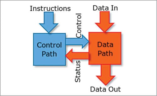
Data path shown in Fig. 1 has data input, control word input, status word output and data output. Width of data word is specified in bits. For our designs we have a generic that stores data width and can be altered globally.
Important components of data path include multiplexers, data bus, arithmetic and logic unit (ALU), barrel shifter, multiplier, register file, universal shift register and output buffers.
Digital circuits can be classified into combinational circuits, sequential circuits and state machines. Data path components are combinational and sequential circuits but not state machines. Combinational circuits do not have the sense of passing time simply because these do not have memory. Their outputs depend on the current values of inputs only.
Sequential circuits have the sense of passing time and time-based ordering of operations. These have memory. Their outputs depend on current and previous values of inputs and previous values of outputs. Sequential circuits have clock and all state changes are synchronised to clock edges. Multiplexer, data bus, ALU, multiplier and buffer are combinational circuits. Register file, barrel shifter and universal shift register are sequential circuits.
Data path architecture
Fig. 2 shows data path architecture. Control, status and address lines for various blocks are not shown. Data bus is a multibit interface to which drivers are connected through their output buffers. Inputs of various blocks can be directly interfaced to the data bus. Here the width of the data bus is a generic called ‘width.’
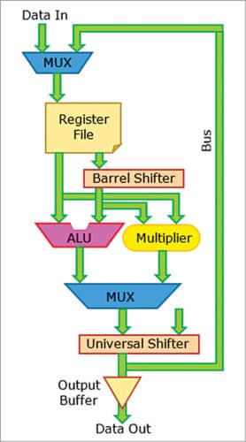
Two multibit 2:1 multiplexers are used: One is used to select between Data In and the computed result from data path output, to be written into register file. The other is used to select one of the outputs from ALU and multiplier as data path output.
Register file is a set of local registers used by data path. There is one input and two output ports. The two outputs are the two input operands to the ALU or the multiplier. The input is used for writing to one of the registers. Write register is selected by the write address and two read registers are selected by the two read addresses.
One of the two operands passes through a barrel shifter. Barrel shifter shifts the bits by specified count to left or right. The new bits on the left or the right are 0s or rotate around of the word.
The two operands beyond barrel shifter are passed on to the ALU and the multiplier as inputs. The ALU is capable of one of the eight operations. The multiplier multiplies two operands and provides the multiplexed output.
The output of the second multiplexer moves to the output universal shifter. The universal shifter is capable of bit-wise left and right shift, serial-to-parallel conversion and multiplexing the output with a second input word. Output buffer at the output of data path provides an interface to the bus. This is required in case multiple data paths drive the output bus.
The various parts included in Fig. 2 are discussed along with VHDL codes in the following sections.
Synthesis tool
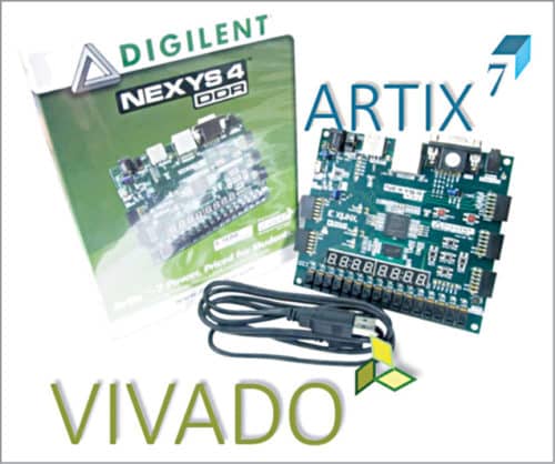
Xilinx Vivado is used as the synthesis tool (Fig. 3). It manages design, synthesis, implementation and device configuration. The flow is as follows:
1. Create a project and select Artix 7 FPGA that you wish to use
2. Add source files for designs
3. Simulate designs and validate results
4. Synthesise designs
5. Specify the input/out (I/O) constraints and generate xsd files
6. Re-synthesise designs
7. Implement designs
8. Generate bit (configuration) files for the device
9. Open (connect through UART) the device connection
10. Configure the device using bit files
11. Validate designs using switches and LEDs of the board
Multibit buffer
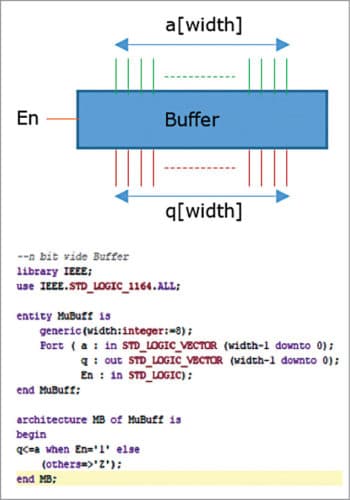
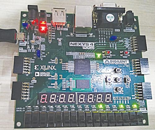
Fig. 4 shows a multiple-bit buffer along with MuBuff.vhd code. The output assumes the same value as the input if En is high. Else, output bits are high impedance. You can see the 1’s and 0’s bits on the LEDs. Fig. 5 shows its implementation on the Nexys 4 board.
Multiplexer
The multibit 2:1 multiplexer can be designed using two multibit buffers. Fig. 6 shows a 2:1 multiplexer. Fig. 7 shows package definition with buffer as component. The hierarchical style code for the multiplexer is shown below (MUXnbit2to1.vhd.):
— n bit 2:1 mux using tristate buffers
— MUXnbit2to1.vhd
library IEEE;
use IEEE.STD_LOGIC_1164.ALL;
library upcomp; use upcomp.SubComp.all;
entity Muxnbit2to1 is
generic(width:integer:=8);
Port ( I0,I1 : in STD_LOGIC_VECTOR
(width-1 downto 0);
q : out STD_LOGIC_VECTOR (width-1
downto 0);
sel : in STD_LOGIC);
end Muxnbit2to1;
architecture Mnb221 of Muxnbit2to1 is
signal nsel:STD_LOGIC;
begin
nsel<=not sel;
TB1:MuBuff generic map(width) port
map(I0,q,nsel);
TB2:MuBuff generic map(width) port
map(I1,q,sel);
end Mnb221;
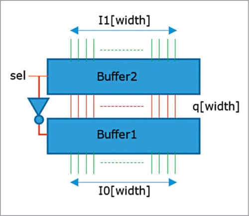

All the components in the project are added to upcomp library; SubComp is a package in the library that has declaration of all the components for hierarchical designs. The complete SubComp.vhd code is included in EFY DVD of this month. The code is simulated, synthesised, implemented and validated on the Nexys 4 board.
Barrel shifter
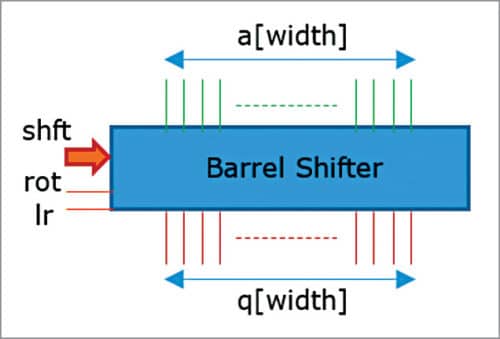
Barrel shifter is a shift register that can be designed using multiplexers. Fig. 8 shows a barrel shifter. Bits shift to left or right by the count fed as shift word. LSB bits are fed with 0’s when rot bit is low and wrapped around from MSB when rot bit is high. The behavioral description of the barrel shifter is implemented in BarrelShifter.vhd.
ALU
Arithmetic and logic unit is the heart of data path. It performs one of the multiple arithmetic and logic operations selected by the select lines. Table I shows various operations that the ALU performs on two operands ‘a’ and ‘b.’ Subscript ‘i’ represents the i-th bit. Inputs ‘a’ and ‘b’ are transformed into ‘x’ and ‘y’ as per the table. Intermediate bits ‘x’ and ‘y’ are fed into multibit full adder. Full adder is designed using half adders.
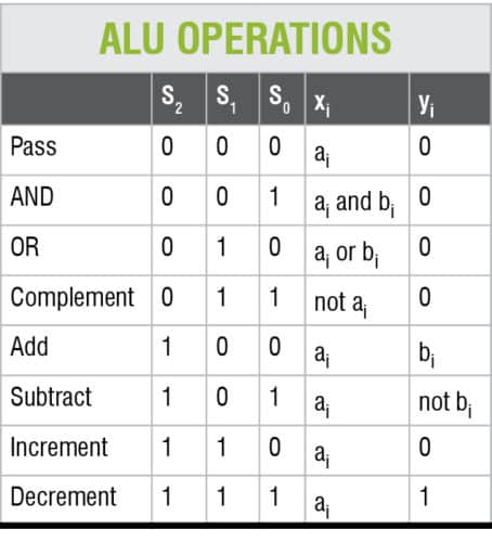
The Transform1bit.vhd code explains bit transformation circuit as per the truth table in the table. The ALU is designed using full adder and bit transform circuit. The code implementation is given in ALUnbit.vhd.
For opcode as 101, the ALU also acts as a comparator. If equ=1 and agb=1, ‘a’ and ‘b’ are equal. If equ=0 and agb=1, ‘a’ is greater than ‘b.’ If equ=0 and agb=0, ‘a’ is less than ‘b.’ The logic also holds for signed numbers.
Fast multiplier
Digital signal processing (DSP) requires fast multiplication of two numbers. If both the numbers are of certain width, the result of multiplication is twice the width. This requires two words that represent lower and higher significance. The output can be multiplexed.
The Multiplier.vhd code below shows VHDL code for the multibit multiplier:
library IEEE;
use IEEE.STD_LOGIC_1164.ALL;
library upcomp; use upcomp.SubComp.all;
entity Multiplier is
generic(width:integer:=8);
Port ( a,b : in STD_LOGIC_VECTOR
(width-1 downto 0);
OP : out STD_LOGIC_VECTOR (width-1
downto 0);
S0 : in STD_LOGIC);
end Multiplier;
……………………………
……………………………
end FM;
Universal shifter
The output of the multiplier or ALU is forwarded through a multiplexer to universal shift register. Universal shift register is capable of bit-by-bit left and right shift with or without rotate option. The basic unit of a register is a D-type flip-flop with asynchronous clear. The code below shows a D-type flip-flop with asynchronous clear:
— D flip flop with clear—DFlipflop.vhd
library IEEE;
use IEEE.STD_LOGIC_1164.ALL;
entity Dflipflop is
Port ( d,clk,clr : in STD_LOGIC;
q :inout STD_LOGIC:=’0’);
end Dflipflop;
architecture DFF of Dflipflop is
begin
q<=’0’ when clr=’1’ else
d when (clk’event and clk=’0’ and
clr=’0’) else
q;
end DFF;
The shift register also needs 2:1 and 4:1 multiplexers. The code below shows a 2:1 multiplexer:
— 2:1 MUX—MUX2to1.vhd
library IEEE;
use IEEE.STD_LOGIC_1164.ALL;
entity MUX2to1 is
Port (I0,I1,S0 : in STD_LOGIC;
q : out STD_LOGIC);
end MUX2to1;
architecture MUX221 of MUX2to1 is
begin
q<=I0 when S0=’0’ else
I1 when S0=’1’ else
‘Z’;
end MUX221;
The code below shows a 4:1 multiplexer:
–4:1 MUX—MUX4to1.vhd
library IEEE;
use IEEE.STD_LOGIC_1164.ALL;
entity MUX4to1 is
Port (I0,I1,I2,I3,S0,S1 : in STD_
LOGIC;
q : out STD_LOGIC);
end MUX4to1;
architecture M421 of MUX4to1 is
signal sel:STD_LOGIC_VECTOR(1 downto 0);
begin
sel<=(S1,S0);
q<=I0 when sel=”00” else I1 when
sel=”01” else
I2 when sel=”10” else I3 when
sel=”11” else
‘Z’;
end M421;
The UniShiftReg.vhd code implements VHDL code for universal shift register.
Register file
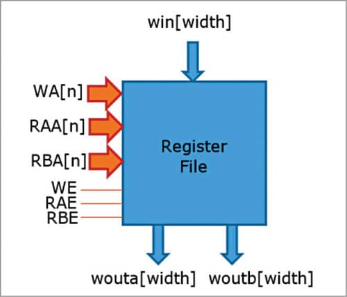
Data path has a set of addressable registers whose control signals and input and outputs are interfaced to common input and output ports, respectively. Such a set is referred to as register file. Width of the register is set by generic ‘width.’ Address width is ‘n,’ resulting in 2n=m registers. There is one input port and two output ports (Port A and Port B). Write address chooses the register to which input word is written at the falling edge of the clock. Write address is decoded by the address decoder. Port A receives the output of the register referred to by Port-A address. Port B receives the output of the register referred to by Port-B address. Two address decoders are used to read a word. Each register consists of multiple D-type flip-flops. D-type flip-flop is modified to include Enable signal that gates the clock input. The DFFEn.vhd code implements D-type flip-flop with Enable signal.
Address decoder has ‘n’-bit-wide input and 2n=m bit output. All the output bits are ‘0,’ except the one referred to by the input, which is ‘1.’ The AddrDec.vhd code implements VHDL code for the address decoder.
Multiple D-type flip-flops can be used to store a word. Such a circuit is referred to as the register. The Reg.vhd code implements VHDL code for a register. Block diagram of the register file is shown in Fig. 9. The RegFile.vhd code implements VHDL code for register file.
Data path integration
Now that you have all the components of a data path as per Fig. 2, write a structural-style VHDL code for data path as given below:
–Data Path –DataPath.vhd
library IEEE; use IEEE.STD_LOGIC_1164.
ALL;
library upcomp; use upcomp.SubComp.all;
entity DataPath is
………………………………
………………………………
end DP;
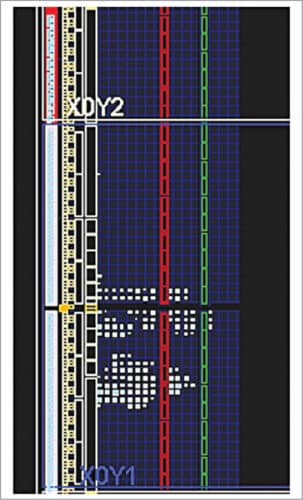
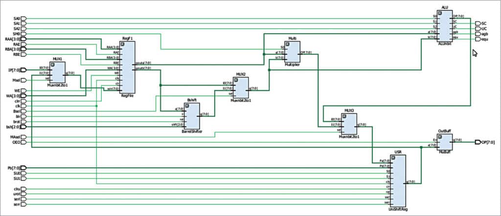
Fig. 10 shows the implementation of data path on FPGA. Fig. 11 shows the schematic of data path.
Data path testing
Data path requires a large number of I/Os, which Nexys 4 board does not support. This requires Virtual I/O and logic analyser IP integration into the project. Further development of a processor is beyond the scope of this article, but interested readers can refer to related material on the Internet.
This article introduced the readers to data path design of a microprocessor. The architecture is open to modifications and readers can come up with innovative ideas to implement data paths for modern microprocessors.
Download source code


