


 Many embedded systems these days need +5V power supply with some special functions such as power-fail detection, zero-crossing signals for mains power supply and possibility to maintain the charging of built-in batteries.
Presented here is the circuit of such a power supply for embedded systems. It provides +5V, battery charger, zero-crossing signals and power-fail signal. The circuit is based on popular low-cost components. It needs simple adjustment with potmeter POT1 to immediately get you started.

Circuit and working
The circuit shown in Fig. 1 is built around a step-down transformer (X1), two bridge rectifiers(BR1 and BR2), adjustable voltage regulator LM317 (IC1), 5V voltage regulator 7805 (IC2), hex inverter Schmitt trigger 74HC14 (IC3) and a few discrete components.
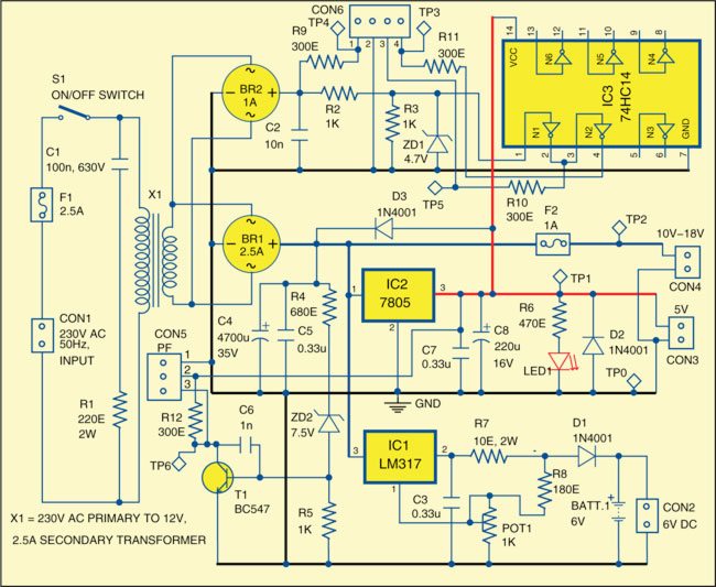
The mains power supply 230V AC, 50Hz is applied to connector CON1. Fuse F1 protects the input from overloads. Resistor R1 and capacitor C1 filter some of the noise coming from the mains power supply. The secondary of power transformer X1 is 12V, 2.5A.

CON3 provides +5V, 1A power supply using standard 5V regulator IC2. Rectifying bridge BR1 is of 2.5A. The value of the main filtering capacitor (C4) should be at least 4700 µF. IC2 provides regulated +5V with output current up to 1A. If a higher current is needed, regulators like 78T05 (3A, 5V) or 78S05 (2A, 5V) can be used. In practice, it is better to limit the load for 78XX up to around 0.7-0.8A. The unregulated output at CON4 provides voltage of 10V to 18V depending on the transformer used and the current consumption from the power supply. This unregulated voltage can be used for peripheral functions. Fuse F2 is used to protect the output.
The power supply incorporates battery charger with adjustable regulator IC1. A 6V rechargeable battery is used to provide power supply to some parts of the system when the mains power supply does not function properly. The maximum voltage level across the rechargeable battery is adjusted using potmeter POT1. The maximum charging current is limited by resistor R7. Regulator IC1 can provide output voltage of +1.25V to +8.2V, adjustable with potmeter POT1.
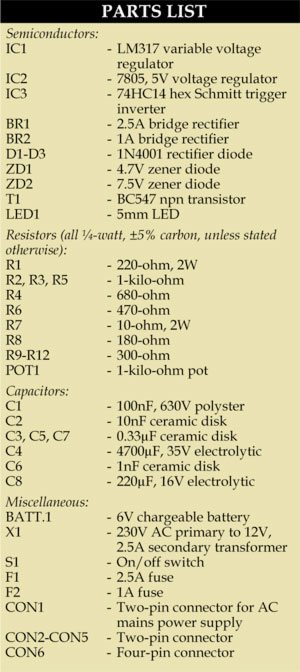
Diodes D1, D2 and D3 protect regulators IC1 and IC2. Bridge rectifier BR2 is used only to provide signals around the zero crossings. Capacitor C2 should have a small value. It is intended to cut only the very high frequency, not to filterthe mains power supply. The values of R2 and R3 can be changed depending on IC3 and parameters of the produced pulses.
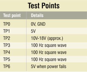
CON5 provides power-fail signal when the voltage at test point TP2 falls below approximately 8V. Transistor T1 stops conducting and the control unit is intimated the same by a high signal at pin 3 of CON5.
The threshold voltage of the power-fail signal is regulated with zener diode ZD2 (7.5V) and resistors R4 and R5. Transistor T1 should preferably be switching type, but most of the npn silicon transistors with a high gain will also work well.
The outputs from pins 2, 3 and 4 of connector CON6 provide different signals with a frequency that is double the frequency of the mains power supply (100 Hz). These signals are active near zero crossings of the mains power supply and can be used for several purposes, such as:
1. The control unit can use them to measure the frequency of the mains power supply.
2. These can be used to synchronise the operation of the control unit with zero crossings of the mains power supply.
3. Тhe amplitude of signal TP4 is proportional to the secondary voltage of the transformer. The control unit can measure it and determine the secondary voltage of X1.
4. Outputs TP5 and TP3 are TTL- or CMOS-compatible depending on IC3. IC3 can be CMOS or TTL; e.g., 74HC14, 74HCT14, 74LS14, etc. It should have built-in Schmitt trigger.
Construction and testing
Use individual heat-sinks for IC1 and IC2. The size of the heat-sink should be calculated according to the dissipated heat for each particular case; e.g., the thermal resistance should be below 5°C/W for each heat-sink. The metallic part of 7805 is connected to the ground pin, while the metallic part of LM317 is connected to the output pin.

Download PCB and component layout PDFs: click here
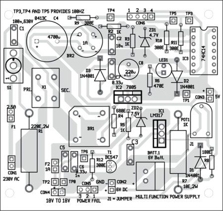
An actual-size, single-side PCB for the multifunction power supply is shown in Fig. 2 and its component layout in Fig. 3. After assembling the circuit on a PCB, enclose it in a suitable case. Fix all the connectors at the rear side of the cabinet for connecting the mains and taking the outputs.
To test the circuit, switch on switch S1 and check various voltages as indicated in the test-points table. LED1 indicates the availability of 5V.
EFY note. Care must be taken while handling the high-voltage section of power transformer X1 as it is connected to the mains power supply.
The author has worked as a researcher and assistant professor in Technical University of Sofia (Bulgaria) and as a lecturer in Kingdom of Morocco. Now he is an electronics engineer in the private sector in Bulgaria
