


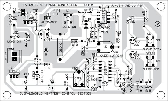
Unless the cause of overload is traced and fault removed, you will not be able to switch on the load. Once the overload fault is rectified, you can switch on the load by momentarily pressing switch S2 (if link JS is kept open) or by pressing RESET switch S4 (if link JS is kept closed). Push switch S3 is provided to manually switch off the circuit by setting the output of bi-stable N1 high.
A single comparator (N3) is used for battery voltage monitoring. With link JS closed, it monitors the battery-voltage and switches the load off when the battery voltage falls below 11.25V and switches it on again when the battery voltage reaches 12.75V in accordance with the set points as referred in Fig. 2.
Regulated 5V DC, used as reference volt-age, is applied to the inverting pin of comparator N3. A proportionate sample of the battery volt-age is applied to the non-inverting pin of comparator N3 via potmeter VR2. At 12V battery voltage, the potmeter is set to provide 5V at the non-inverting pin. With the component values selected, you get the required switching on/off threshold points of 5V±0.325V, which corresponds to the battery voltage of 12V±0.78V or a cut-off voltage level of 11.22V and switch-on level of 12.78V. Those interest-ed in the mathematical analysis may follow the relationships given in Fig. 7.

The output of comparator N2 is used for load-off indication. It lights up LED2 when the load is cut-off. The outputs of N2 and N3 form a wired-OR junction. Thus if any of these comparator outputs is low, the output at the junction point is low. Conversely, both the outputs need to be high so that the output at the junction is high.
Overload-current comparator N1 acts as a bistable latch. Hence once set to high state due to overload, the reset button (switch S4) must be pressed to reset it after removal of any fault that caused the overload. To drive the MOSFET (T4 in Fig. 5), a high rate of change of current for gate drive is needed. Hence the wired-OR output of comparators N2 and N3 is passed through Darlington transistor T5 for driving MOSFET T4 connected at point D.

PWM charging circuit. Commonly available PWM controller IC TL494, which is widely used in PC SMPS and costs less than an ordinary op-amp, is used for this circuit.
PWM on/off circuit. Error amplifier-2 is employed as enable/disable control to cut off the PWM output of TL494 when the battery voltage reaches the upper set limit of 14.3V (13.8V+0.5V) and enable it again when the battery reaches the lower set limit of 13.3V (13.8V–0.5V). This function is realised with the help of the circuit shown in Fig. 8. The first comparator provides the necessary cut-off/cut-on points, while the second comparator is used as a simple inverter. Necessary formulae and parameters used for design are shown in Fig. 8 itself. This circuit is interfaced to error amplifier-2 of TL494 after integration with temperature compensation.
Temperature-dependant reference voltage generation circuit. A careful look at Fig. 8 shows that VREF has been obtained from a temperature-dependant reference volt-age (9.2V at 25°C) and one-third of the average VBATT value has been used for comparison with VREF. Variation of VREF shifts the upper and lower threshold points used for switching on/off the PWM output. The circuit used for generation of temperature-dependant reference voltage is shown in Fig. 9.
We had earlier stated that for a 12V lead-acid battery, a 30mV/°C negative temperature correction is required to be applied for the battery voltage set points as shown in Fig. 2. The average charging volt-age at 25°C is indicated as 13.8 volts. This means that the average charging voltage at 0°C should be higher by 0.75V (30mV ×25) or it would be 14.55V (13.8+0.75) at 0°C.
National Radio’s LM35DZ temperature sensor IC provides 10 mV/°C. It is one-third of 30 mV/°C required for correction of the 12V battery. Thus we use one-third of the battery voltage (14.55/3=4.85V) as reference voltage at 0°C and subtract from it 10 mV/°C using a DC difference amplifier formed from LM358 IC as shown in Fig. 9. The 4.85V is derived from 5V reference (generated by TL494 IC) using a resistive divider. This circuit provides a temperature-corrected reference voltage of 9.7V at 0°C (or 9.2V at 25°C and so on). This reference output voltage is two-third the battery charging voltage at any given temperature. It is halved (4.6V)using a resistive divider in Fig. 8. Thus the resultant reference voltage equals one-third of the average battery charging voltage at a given temperature. Accordingly, the battery voltage is also divided by ‘3’ before application to the main PWM circuit configured around TL494 IC (Fig. 10).
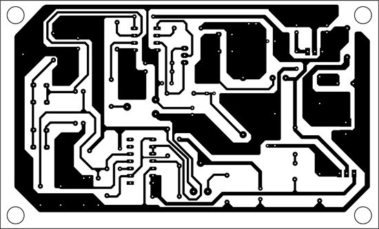
Fig. 15: An actual-size, single-side PCB for the pwm control circuit shown in Fig. 10

very useful article for both student and electronics professional.