Download PDFs and component layout PDFs: click here
Input of hysteresis circuit of Fig. 9. Thus we uniquely produce temperature-compensated set points for enabling/disabling the PWM output. (Note that the temperature sensor should be positioned in the vicinity of the battery to measure its temperature and the output from the temperature sensor to the differential op-amp should be conveyed using a properly grounded (both ends) 75-ohm coaxial cable.) Circuits shown in Figs 8 and 9 have been integrated into the main PWM circuit (Fig. 10) configured around TL494 IC.
PWM error-amplifier circuit. PWM control is exercised through error amplifier-1 of TL494. The gain of error amplifier-1 is fixed at 100 using feedback resistor R39 of 51 kilo-ohms, while resistor R38, in series with reference voltage of 5V, is selected as 510 ohms. The sample voltage is derived from the battery using a resistive divider comprising resistors R35 and R36 to provide 5V for the non-inverting terminal of error amplifier-1, corresponding to the maxi-mum battery voltage limit of 14.3 volts.
The output of TL494 is configured for single-ended operation by grounding its control pin 13. The common emitter output developed across R51 is fed to the totem-pole amplifier comprising complementary Darlington pairs of transistors T8 and T9 for driving the MOSFET connected at point ‘C’ in Fig. 5. The various circled points in Fig. 10 are connected to identical points in Fig. 5. This completes the description of the complete PV charge controller circuit.
An actual-size, single-side PCB for the main charger circuit of Fig. 5 is shown in Fig. 11 and its component layout is shown in Fig. 12. Various points for connections to other circuits are shown with encircled alphabets A through G.
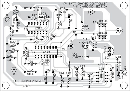
The actual-size, single-side PCB for the over-load cum low-battery load disconnect circuit of Fig. 6 is shown in Fig. 13 and its component layout in Fig. 14. The actual-size, single-side PCB for the PWM control section of Fig. 10 is shown in Fig. 15 and its component layout in Fig. 16. Before you start charging the battery, all the connecting points, as indicated in the PCB layout as per the schematic diagrams, should be connected to respective points A through H. The LM35DZ temperature sensor should be attached to the battery (to be charged) using quick fix glue by extending the connection from the PCB (Fig. 16) to the battery using coaxial cable.
The author is ex-Technical Editor, EFY magazine, and author of some very interesting books


very useful article for both student and electronics professional.