In most of the modern manufacturing and processing industries, there is complete industrial automation through sophisticated hardware and software like programmable logic controller (PLC), distributed control system (DCS), and supervisory control and data acquisition (SCADA). Microcontroller-based embedded systems play major role in industrial automation. One such widely used system is the programmable timer. The major applications of programmable timer are as follows:
1. Initiating the process after de-sired time
2. Switching on/off the process after predetermined time
3. Providing delay in between processes
4. Applying input to on/off type open-loop control system
Depending upon the requirement of process, one can set the time of programmable timer. As the time period expires, the timer will either trigger or shut the process. Earlier there were mechanical timers that used gear assembly (same as wall clock) and mechanical contacts. But the problem with these was that due to mechanical parts and movements, they were not durable. Electronic timers have become very popular as these have more functionalities and long operating life.
A simple electronic timer can be made using a single IC 555 in monostable mode that can switch on/off the process after desired time. Also, in chain process (where the end of first process starts second process and so on), one can use a number of such monostable blocks to make a sequential timer. But these circuits do not include additional features like digital display, system failure indication, remote operation and alarms. Since the precision and accuracy of these timer circuits depend upon the value of the resistor-capacitor components that may deviate, we might not get the exact and precise timing. To enhance the programmable timer for generating precise timing and additional features, microcontrollers (embedded controllers) are used with peripheral devices.
Some of the features of programmable industrial on/off timer presented here include:
1. Time set from 1 to 60 seconds (can be extended)
2. ‘On’ time and ‘off’ time can be programmed (from 1 to 60 seconds)
3. Repeat (continuous) and single operation
4. Fully remote-controlled within 100-metre range
5. User-friendly front-panel controls and display panel with LCD
6. Emergency stop buttons (on control panel as well as on remote)
7. Provision of potential-free relay contacts for connecting any 230VAC at 10A or 28V DC at 10A device/application
Circuit description
The complete hardware circuit is divided into two sections—programmable timer main circuit and remote control transmitter and receiver units. The main circuit is a fully-functional standalone unit with front-panel control switch and LCD display. Remote control transmitter and receiver are add-on units. The receiver outputs are connected with respective control input pins of main circuit. Receiver output facilitates user to program and control timer operation using remote within 100-metre range.
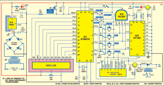
Main circuit. Fig. 1 shows the circuit diagram of industrial on/off timer. The circuit comprises microcontroller AT89C51 (IC1), LCD, transistors and a few discret components. The data pins D0 through D7 of LCD are connected with port pins P2.0 through P2.7 of microcontroller AT89C51. The control pins register select (RS), read/write (R/W) and enable (E) are connected with port P3 pins P3.0, P3.1 and P3.2, respectively. Preset VR1 is connected with pin 3 of LCD for contrast control. Switches S1 through S4 are connected to port pins P1.0 through P1.3 by 4PDT toggle switch S8. Two single-pole double-throw (SPDT) switches S6 and S7 are connected at P3.5 and P3.6. Switch S6 selects for either remote or keypad control, and switch S7 selects control for either repeat or single mode operation. Port pin P3.7 drives relay through transistors T1. Diode D5 acts as free-wheeling diode for relay RL1.
Power-on reset is provided by the combination of resistor R1 and capacitor C3. Switch S5 is used for manual reset or emergency stop function. A 12MHz quartz crystal along with two 33pF capacitors provides clock pulse to the microcontroller AT89C51.
The 230V, 50Hz AC mains is stepped down by transformer X1 to deliver a secondary output of 12V, 500mA. The transformer output is rectified by a full-wave rectifier comprising diodes D1 through D4, filtered by capacitor C4 and regulated by IC 7805 (IC4). Capacitor C5 bypasses the ripples present in the regulated supply. LED1 acts as the power indicator and R7 limits the current through LED1.
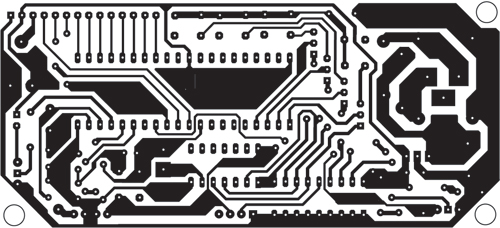
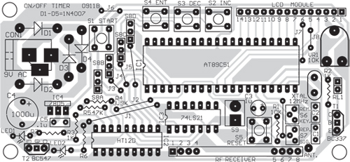
An actual-size, single-side PCB for the programmable industrial on/off timer is shown in Fig. 2 and its component layout in Fig. 3. Assemble the circuit on a PCB as it minimises assembly time and errors. Carefully assemble the components and double-check for any overlooked error.
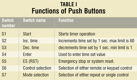
Operation. The functions of all keys are given in Table I. The mode selection switch S7 selects either repeat or single mode. Single mode allows user to run the timer operation in ‘on’ time and ’off’ time sequence once. In repeat mode of operation, the timer repeats ‘on’ time and ’off’ time sequence continuously. During this cycle if this switch is changed to single-mode, the timer stops as the cycle completes. Also, if the emergency stop (ES) button is pressed during any mode of operation the timer operation will stop.
The step-by-step operation when the main circuit is powered is as follows:
1. The ‘enter on time’ message is displayed on LCD
2. User has to enter the desired time by incrementing/decrementing time using ‘Inc.’ (S2)/’Dec.’ (S3) keys
3. After pressing the ‘Enter’ (S4) key the user will be prompted to enter ‘off’ time
4. Using the same S2 and S3 keys, the ‘off’ time may be entered and the ‘Enter’ key pressed
5. ‘Press Start’ message is displayed as the user enters the time
6. After pressing ‘Start’ (S1) key the operation starts
7. The relay is energised and the device remains on till the ‘on’ time counts down to 0. After that the relay is de-energised and the device turns off. It remains in this state till ‘off’ time counts down to 0
8. If the timer is operating in the repeat mode the cycle will repeat continuously and device will be switched on and off after required time intervals. In this mode if the operation has to be stopped then either switch S7 has to be toggled or ES button has to be pressed
9. If the timer is operating in single mode then as one on-off time cycle completes, the timer stops working. One has to enter ‘on’ time and ‘off’ time again to re-start operation
10. For remote control operation, port pins P1.0 through P1.3 of microcontroller AT89C51 are changed to D11 through D8 of HT12D, respectively, using four-pole double-throw (4PDT) switch S8. Also, switch S6 connected to port pin P3.5 is changed to remote position to set re-mote operation mode.
Remote control transmitter and receiver circuit. Remote control transmitter and receiver are made using readily available encoder (HT12E) and decoder (HT12D) chips.
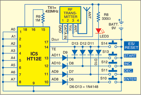
Transmitter circuit. Fig. 5 shows the circuit diagram of transmitter consisting of two main components—encoder HT12E (IC5) and radio frequency transmitter module 433MHz (TX1). All the address pins A0 through A7 are tied to ground to set address ‘00h.’ A one mega-ohm resistor is connected between oscillator pins 15 and 16 of HT12E. DOUT pin17 of HT12E is connected with input of ASK transmitter (TX1). Switches S10 through S13 are connected with data input pins AD8 through AD11 of HT12E in such a way that when you press any key, TE pin is automatically grounded. Key S14 is directly connected between TE pin and ground as shown Fig. 5. LED3 is connected for indication of pressing the switch. An actual-size, single-side PCB for RF transmitter is shown in Fig. 6 and its component layout in Fig. 7.
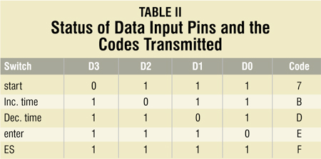
Operation. When you set the address and data inputs on HT12E and pull down TE pin low, that address and data are serially transmitted through DOUT pin 17 of HT12E. Here the address is already set to ‘00h.’ Now as any key is pressed, respective data pin goes low and TE pin is grounded. Status of data along with 8-bit address is serially transmitted through ASK transmitter. ASK transmitter modulates these data signal with 433MHz carrier and transmits it through antenna. Table II shows the status of data input pins and the codes transmitted for a particular switch.
Receiver circuit. Receiver circuit is included in Fig. 1. All the address pins of decoder HT12D (IC2) are connected to ground to set same address ‘00h’ as on the transmitter. Data output pins D8 through D11 are connected to microcontroller (IC1) through contacts of 4PDT switch S8. Also, all four outputs are given as input to 4-input AND gate. The output of AND gate is connected to reset input pin 9 of microcontroller AT89C51 of main circuit. VT pin of HT12D drives LED2 through transistor T1 for indication of data reception. A 51-kilo-ohm resistor is connected between oscillator pins 15 and 16 of decoder HT12D. Output signal of ASK receiver (RX1) is connected with DIN pin 14 of HT12D.
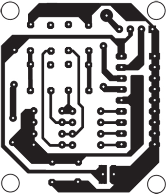
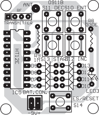
Download PCB and component layout PDFs: click here
Operation. ASK receiver receives 433MHz carrier signal and demodulates the address and data before giving it to decoder HT12D. HT12D receives these bits serially through DIN pin 14 and compares the address. If received address and set address match, the data will be latched on pins D8 through D11 of decoder HT12D. The VT pin 17 becomes high momentarily as data is latched. This is indicated by LED2. If AD11 pin goes low by pressing start switch (S1) of the transmitter side, only D11 pin 13 at the receiver side becomes low and all other pins become high. Since D11 pin is connected to port pin P1.0 of microcontroller AT89C51, it gives the start signal. Data is received similarly for D8, D9 and D10. When ES key is pressed all data pins D8 through D11 are high. So at the receiver side all the pins become high. That makes the output of AND gate high, which is given to the reset pin 9 of microcontroller.
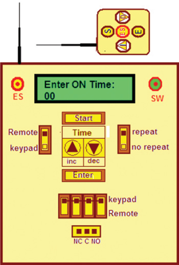
Because there is a latch action at D8 through D11 outputs, all A through D inputs to AND gate remain high till any other key is pressed at the transmitter. This will continuously apply reset signal to microcontroller AT89C51. To remove reset condition, one SPST (S9) is used in between to make and break the direct connection. Open switch S9 will break the connection and reset pin will not get high logic from the AND gate. Now, after starting the operation, to activate ES from remote, press the switch again to make the connection. Fig. 8 shows the proposed arrangement for front panel and remote control for industrial on/off timer.
Software
The program is written in ‘C’ language and compiled through Keil µVision4 compiler. The program is well-commented and easy to understand. Complete program is divided in twelve different functions. Out of these twelve functions, four functions are for LCD handling, four for timer operation, two delay functions, one interrupt function and the last one is the main function.
LCD handling functions. The various functions are as follows:
‘writecmd’ function. It sends command byte to LCD by taking one argument byte that is sent to port P0
‘writedata’ function. It sends data byte to be displayed on LCD. It also takes one argument byte and sends it to P0
‘writestr’ function. It writes the whole string (message) on LCD taking pointer as an argument that points address of first character of string. Through the pointer it sends all the characters one by one to port P0
‘busy’ function. It checks the status of busy flag of LCD. If the flag is set that means LCD is not ready and pro-gram remains within loop. When flag is reset that means LCD is ready and program comes out of loop
Delay functions.
‘keydly’ function. It generates key debounce delay of around 0.1 second using ‘for loop’ statement twice
‘dly1sec’ function. It generates approximately one second delay using ‘for loop’
Interrupt function.
‘takeinput’ function. This interrupt function handles external interrupt1. It just saves the status of port P1 whenever external interrupt1 occurs
Timer operation functions.
‘Start’ function. It starts the timer operation by sending high logic to port pin P3.7 and energising the relay. The countdown time is displayed on LCD as ‘Device ON.’ Then it sends low logic to port pin P3.7 and de-energises the relay. Again countdown time is displayed as ‘Device OFF.’ It then checks the status of port pin P3.6. If it is high the cycle repeats continuously and if it is low the operation stops
‘Inctime’ function. It increments ‘ontime’ or ‘offtime’ variables till maximum limit (60 second) is reached. To display the variable on LCD the value must be in ASCII format. So first two digits are separated and then converted into equivalent ASCII values using array named ‘ascii.’ This array includes ASCII values of all 0 to 9 digits
‘Dectime’ function. It is similar to ‘Inctime’ function. The difference is that it will decrement ‘ontime’ or ‘off-time’ variable till minimum limit (1 second) is reached
‘Enter’ function. It changes the messages on LCD as ‘Enter OFF time:,’ ‘Press Start,’ etc. It is also used to enter ‘ontime’ and ‘offtime’ variables, alternatively.
Main function. It first initialises LCD and then displays message ‘Enter ON time:.’ It then checks the status of port pin P3.5 of microcontroller. If port pin P3.5 is high, it means timer operation is controlled through keypad and if it is low the timer operation is controlled through remote. It waits in continuous loop till any key is pressed from keypad or remote. As the key is pressed, the function is detected and it calls the particular function corresponding to that key like ‘Start,’ ‘Inctime,’ ‘Dectime’ or ‘Enter.’
Download source code: click here
The author is lecturer in electronics and communication in EC engineering department, Government Polytechnic, Amreli


kindly let me know how to extend the time limit of this circuit
You can change it in the source program at the line if(offtime<60) offtime++;
denemek isterdim kaynak kodunu bulamadım teşekkürler
Sevgili cahit , bizim kaynak web sitesi ile bazı sorunlar yaşıyoruz . o çözüldüğünde , kaynak kodu ile sayfa güncellenecektir.
sir please send the hex code of Programmable Industrial On-Off Timer With RF Remote
Source Code Download link is broken It shows “Page not found”
Thank you, Krishna for your comment. We have updated the link.
We have updated the article with the correct code.
Source code link not available
Kindly refresh the page and re-download.
Dear sir,
I tried to refresh not possible option here ,So kindly sent to through my mail [email protected].
Yours kindly
surendaran
Please send link to my mail [email protected]
Thank u so much :)))
You are most welcome.
Hi how to change the program in minutes. How to make a change to see both in min and sec.
Download source code: click here – 404 Not Found ???
Hi, thank you for your feedback. I have added the correct source code. Please refresh the page.