These days there a lot of audio power amplifiers in integrated circuits (ICs). But it is still interesting to produce audio power amplifiers with operational amplifiers (OAs) and with output power bipolar transistors. Some of the reasons for that are listed below:
- The power transistors has much higher power dissipations that the audio ICs
- The power transistors has much higher maximal working voltages and collector currents
- The power transistors have higher maximal working temperature,
- It is simple to replace the power transistors in case of damaging, etc.
Here we will see simple audio power amplifier with the operational amplifier (OA) NE5534/A and two Darlington transistors producing up to 30W of output power. The OA NE5534/A was selected for the circuit because it has maximal working power supply up to +22V, it has significant bandwidth, low THD, high slew rate, output current more than +-20mA, etc.
Description of the circuit
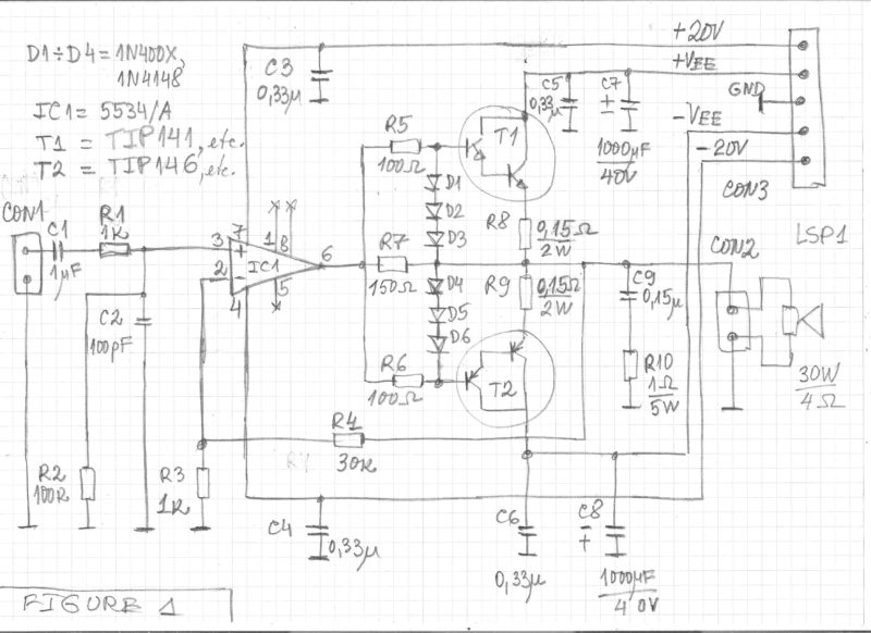
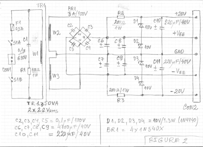
Figure 1 shows the circuit of the audio amplifier and Figure 2 shows the circuit of the power supply.


The audio signal is applied on CON1 of the Figure 1. The capacitor C1 is cutting the DC input signal. R1 and C2 limit the frequency of the input signal. R2=100kOhm determines the input resistance of the amplifier. The gain of the amplifier is determined by the resistors R3 and R4 according to the formula below:
Gain = 1 + R4/R3 = 1 + 30k/1k = 31.
The gain can de set to any appropriate value above 3, because NE5534/A is stable for gain higher than 3. Resistors R5, R7 and R6 reduce the THD of the amplifier. C9 and R10 increase the stability of the amplifier and reduces the THD. The Darlington transistors T1 and T2 amplify the output current of the OA.
Limiting the output current
The amplifier has limiting the output current of the Darlington transistors. The output current should be limited to around 4A. D1, D2, D3 and R8 limit the output current of T1 (npn). D4, D5, D6 and R9 limit the output current of T2 (npn). The diodes D1 to D6 are 1N400X and are mounted on the heat sinks of the output transistors. Here we have R8 = R9 = R are from 0.15Ohm to 0.22Ohm. The maximal output current is calculated with the approximate formula given below:
Imax = 0.65V/R = 0.65V/0.18Ohm = 3.6A or
Imax = 0.65V/R = 0.65V/0.15Ohm = 4.3A
The Output Power
The output power of the amplifier depends on the power supply and the output transistors, the size of heat sinks and the load resistance. The recommended heatink is with thermal resistance below 2C/W. The transitors should be insolated from the heatsink. We can have up to around 30W over a load or 4Ohm. The transistors T1 and T2 should have gain more than 800 at collector current of 4A. The maximal power dissipation of each of the transistors should be preferably more than 40W and the peak output current more than 6A. Several appropriate couples of Darlington transistors are given in Table 1.
| NPN | PNP | Ic | Icpeak | Vcemax | Pdmax |
| TIP141 | TIP146 | 10A | 15A | 80V | 125W |
| TIP142 | TIP147 | 10A | 15A | 100V | 125W |
| TIP121 | TIP126 | 5A | 8A | 80V | 65W |
| TIP122 | TIP127 | 5A | 8A | 100V | 65W |
| TIP101 | TIP106 | 8A | 15A | 80V | 80W |
| TIP102 | TIP107 | 8A | 15A | 80V | 80W |
| 2N6301 | 2N6299 | 8A | 16A | 80V | 75W |
| BD647 | BD648 | 8A | 12A | 80V | 62.5W |
| BD649 | BD650 | 8A | 12A | 100V | 62.5W |
| BD651 | BD652 | 8A | 12A | 120V | 62.5W |
Fwwl interested? Check out other electronics projects.


how c9 and r10 reduce total harmonic distortion?
R4 and R3 are connected such that they form an INVERTING CONFIGURATION… whose gain should be -R4/R3..But it is given 1+R4/R3..
Although C1 will block external DC, it’s a good idea to have a capacitor in series with R3 so any DC offset doesn’t get amplified and appear at the speaker output.
Can you post the PCB layout?