Built on the lines of payphones, here is an automatic coin collection device for payloads like lamps and air-conditioners to be used on a private electrical line. It is useful for paying guest houses, lodges and trains.
The system makes use of a sensor for detecting the coin and a microcontroller that counts the coins and shows the count on a 7-segment display. When you close the load switch provided in the circuit, the relay energises to connect the load and the coin count on display starts decrementing. When the count decrements to zero, the relay de-energises to disconnect the load.
Circuit description
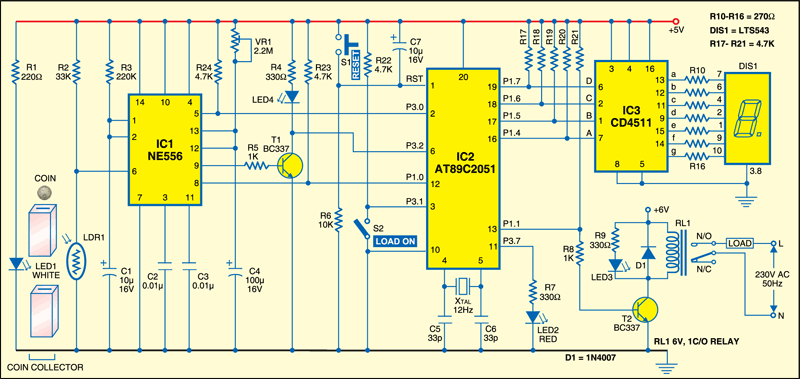
Fig.1 shows the put-coin-and-draw power circuit. It comprises microcontroller AT89C2051 (IC2), dual timer NE556 (IC1), 7-segment decoder CD4511 (IC3), regulators 7805 and 806 (IC4 and IC5), and a few discrete components.

LED1 is used as the light source for light-dependent resistor LDR1, which is made of cadmium sulphide and acts as the coin detector. Resistor R1 limits the current through LED1. The light from LED1 falls continuously on LDR1, whose resistance decreases with increase in the incident light intensity.
The NE556 dual monolithic timing circuit is a highly stable controller capable of producing accurate time delays. It is basically a dual NE555. In the time delay mode of operation, the time is precisely controlled by an external resistor and capacitor. The two timers operate independently of each other, sharing only VCC and ground. The circuits may be triggered and reset on falling waveforms. One timer of NE556 is used for coin detection.
LDR1, connected at trigger pin 6 of IC1, offers low resistance when light is falling on it and its trigger input goes low to set the flip-flop and make output pin 5 of IC1 high.


When a coin is inserted, it interrupts the light falling on LDR1, and trigger pin 6 of IC1 goes high to make output pin 5 low. This high-to-low pulse is used by the microcontroller to display the coin count.
Microcontroller AT89C2051 is the heart of the circuit. It is a low-voltage, high-performance, 8-bit microcontroller that features 2 kB of Flash, 128 bytes of RAM, 15 input/output (I/O) lines, two 16-bit timers/counters, a five-vector two-level interrupt architecture, a full-duplex serial port, a precision analogue comparator, on-chip oscillator and clock circuitry. A 12MHz crystal is used for providing the basic clock frequency. All I/O pins are reset to ‘1’ as soon as RST goes high. Holding RST pin high for two machine cycles, while the oscillator is running, resets the device. Power-on reset is derived from resistor R6 and capacitor C7. Switch S1 is used for manual reset.
Coin-detection output pin 5 of NE556 is interfaced with port pin P3.0 of the microcontroller (IC2). The microcontroller program counts the number of coins inserted and the count is shown on a 7-segment display.
The ‘A’ through ‘D’ inputs of 7-segment decoder IC3 are interfaced with port pins P1.4 through P1.7 of IC2. IC3 accepts the BCD input and decodes it to show on the 7-segment display. Coin detection is also indicated by LED2, which is connected to pin P3.7 of the microcontroller.
After inserting the coin, close load switch S2. Port pin P1.1 of the microcontroller goes high to drive transistor T2 into saturation. Relay RL1 energises and LED3 glows to indicate that the load is now switched on. D1 acts as a free-wheeling diode.
As power is drawn by the load (pin P1.1 high), the count shown on the 7-segment display (DIS1) decrements. Port pin P1.0 of the microcontroller triggers the second timer of NE556. When trigger pin 8 of NE556 goes low, its output pin 9 goes high for a time period decided by preset VR1 and capacitor C4. The high output of the timer is inverted by transistor T1 and fed to port pin P3.2 of the microcontroller (pin 6 of IC2). The count display decrements by ‘1’ after port pin P3.2 of the microcontroller receives five pulses (indicated by glowing of LED4).
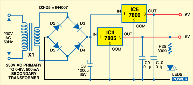
Fig.2 shows the power supply circuit. The 230V AC mains is stepped down by transformer X1 to deliver the secondary output of 9V, 500 mA. The transformer output is rectified by a full-wave bridge rectifier comprising diodes D2 through D5, filtered by capacitor C8 and then regulated by ICs 7805 (IC4) and 7806 (IC5). Capacitors C9 and C10 bypass the ripples present in the regulated 5V and 6V power supplies. LED5 acts as the power-‘on’ indicator and resistor R25 limits the current through LED5.
Construction
An actual-size, single-side PCB for the put-coin-and-draw-power circuit is shown in Fig. 3(View as PDF) and its component layout in Fig.4(View as PDF). Wire the circuit on the PCB and check for proper connections using a multimeter.
Download PCB and component layout PDFs (Fig. 3, 4): click here
Take a 10cm long, hollow, rectangular cuboid of plastic in which a coin can be inserted easily. Drill holes on its opposite sides at the centre and fix LED1 and LDR1 such that these are placed face to face. Align LED1 and LDR1 such that light from LED1 falls on LDR1 directly. Cover the coin-collection assembly to maintain darkness, leaving only coin-insertion and coin-release holes open. Extend LED1 and LDR1 from the PCB to the coin assembly using wires.
When a coin is inserted into the coin-collection assembly, light falling on the LDR is blocked as the coin comes in between LED1 and LDR1. LDR1 offers high resistance in the absence of light and this is detected by one timer of NE556 and indicated by LED2.
You can insert up to nine coins and this count is displayed on DIS1. When you close the load switch S2, the relay energises and the load turns on. The count displayed on DIS1 starts decrementing after LED4 blinks five times. The relay de-energises to turn the load off when the count displayed on DIS1 becomes zero. Load-‘on’ duration can be adjusted using preset VR1. Never insert the coin without pressing reset switch S1.
Software
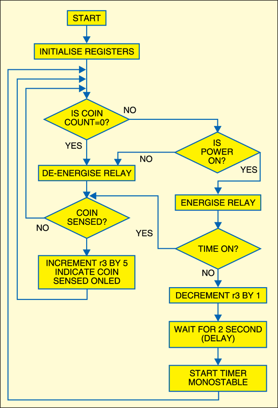
The source program is written in Assembly language and assembled using Metalink’s ASM51 assembler, which is freely available on the Internet for download. The source program has been well commented for easy understanding. It works as per the flow-chart shown in Fig.5.

First, the program initialises the microcontroller’s registers, then it checks whether memory register is zero. If register r3 is zero, it goes for coin detection. Else, it proceeds to count update and display. Coin-counter register r3 is incremented by five after insertion of one coin. When the load switch is closed, port pin P3.1 goes low. Port pin P1.1 goes high to energise relay RL1. Port pin P3.2 goes low five times then display count number decrements by one.
Download the source code and other relevant files: click here


where we get coding for this?
help us
What is the overall cost
sir , please provide me with the code
Sir , I need the coding of this project sir.
Sir, can i get the program for the micro controller plz
Sir can i get the program for microcontroller
can someone provide the code for the micro-controller?
link is down for source code
Kindly give us some time, we are reuploading the code.
The source code is not available, please re-upload it!
Hi, thank you for your comment. We have updated the article with the correct source code link.