


 This article presents a simple circuit to convert transistor-transistor logic (TTL) or pulse width modulation (PWM) signal to analogue signal using LM358 operational amplifier. The circuit can be used as an extension shield for Arduino or microcontroller (MCU) or TTL/CMOS signal generator.
PWM-based digital-to-analogue converters (DACs) are often used to produce analogue signals from digital outputs. Usually, solutions for these PWM-based DACs include three main blocks:
1. Digital PWM generator: Mostly, this employs an MCU or Arduino, but can also use a square-wave generator circuit.

2. Analogue integrator: In the simplest case this can be a single RC network. Sometimes, the signal is for driving an electrical motor.
3. Analogue output buffer or amplifier: It provides necessary output voltage, current and power.

Main advantages of PWM DACs include simplicity, low cost, digitally-controlled resolution up to 10 bits (or more), and the possibility to obtain high output current, voltage and power.
Circuit and working for PWM-To-Analogue Signal Converter
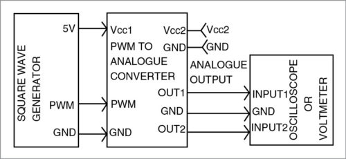
The block diagram of the PWM-to-analogue converter is shown in Fig. 1 and its circuit diagram in Fig. 2. The circuit consists of two parts: input passive RC low-pass filters with three stages and two output stages (OUT1 and OUT2).
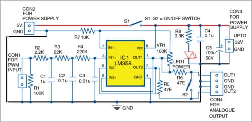
Input passive low-pass filters are built around resistors R2, R3 and R4 and capacitors C1, C2 and C3. Cut-off frequencies at -3db for each of the three stages are calculated according to the formulae given below.
For the first stage,
F1=1/(6.28×R2×C1)
For the second stage,
F2=1/(6.28×R3×C2)
For the third stage,
F3=1/(6.28×R4×C3)
In most cases, F1=F2=F3
where R4=10×R3=100×R2 and R2 510-ohm
Cut-off frequencies at -3db are:
F1=F2=F3=72Hz
You may select any appropriate cut-off frequencies for RC filters. Here, we use 5V power supply of the computer or Arduino at CON2 as voltage reference source for the PWM signal.
Output stages are built around two internal operational amplifiers of IC1. First internal operational amplifier (OA1) is formed by pins 2, 3 and 1 of IC1, and the second operational amplifier (OA2) by pins 6, 5 and 7 of IC1.
On closing switch S2, both operational amplifiers work in parallel over the same load at CON4. On opening it, both produce the same voltage over two separate loads. Preferably, the loads should be above 2-kilo-ohm.
If S1 is closed, you can use the power supply of computer VCC1 like Arduino at CON2. If S1 is opened, you can use power supply VCC2 up to 32V at CON3.
OA1 works as a non-inverting amplifier with the gain (Av1) defined by preset VR1 and resistor R7. Minimum gain is +1, and maximum gain is +11. Gain is set according to requirements using VR1, required output voltage and power supply of IC1. It is calculated using the simplified formula given below.
Av1=1+VR1/R7
OA2 works as a follower, where gain Av2=+1
Construction and testing
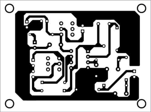
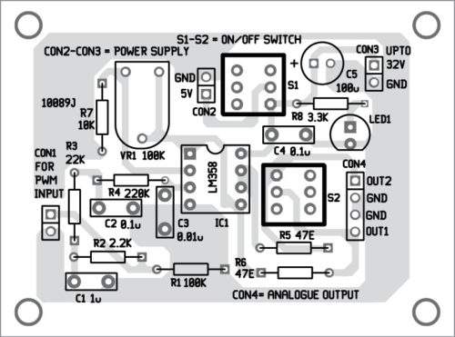
An actual-size PCB layout of the PWM-to-analogue converter is shown in Fig. 3 and its components layout in Fig. 4.
Download PCB and component layout PDFs: click here
Before testing, note that, maximum output voltages (Vout) at OUT1 and OUT2 depend on: power supply of operational amplifiers, position of potentiometer VR1 and output voltage levels of TTL/CMOS output driving the module.
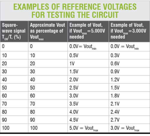
To test the circuit, fix the frequency of PWM (for example, 1000Hz) and change the duty cycle time period TON and TOFF of the pulses. Refer to the table to test output voltages.
Linearity of the conversion depends, to some degree, on the parameters of the digital output. A too low or too high PWM duty cycle should be avoided. Usually, duty cycle of PWM <5% and >95% must be avoided. In most cases, PWM DACs are good for driving LEDs, incandescent lamps, LCD displays, DC motors and loudspeakers, among others.
Spectrum of the rectangular signal produced by the PWM is large and variable. This can be a problem without appropriate filtering, construction and PCB layout. Resistors, capacitors and operational amplifiers for filtering and buffering of PWM signals should have appropriate characteristics. Usually with PWM DACs, you obtain high resolutions but not accuracy.
Petre Tzv Petrov was a researcher and assistant professor in Technical University of Sofia (Bulgaria) and expert-lecturer in OFPPT (Casablance), Kingdom of Morocco. Now, he is working as an electronics engineer in the private sector in Bulgaria.

Can this circuit be used for 0 – 10V output?