

Using integrated load switches simplifies the design and ensures safe and reliable power sequencing while maintaining a compact footprint compared to traditional discrete MOSFET implementations.
In many electronic systems, the proper operation of subsystems and downstream components depends on controlled power-up and power-down sequences. Power sequencing is essential in applications where timing constraints are crucial, as it ensures that each element receives power in the correct order, avoiding potential damage or malfunction. This design is exceptionally versatile, offering the ability to customise timing configurations by adjusting the board’s jumpers, resistors, and capacitors. This flexibility makes it adaptable to various applications, from multi-function printers (MFPs) to set-top boxes (STBs), where precise timing sequences are required for optimal operation.
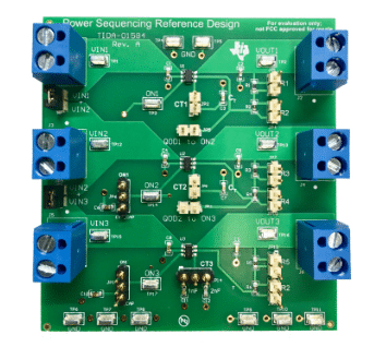
This reference design, TIDA-01584 by Texas Instruments (TI), demonstrates multiple power sequencing configurations using load switches, allowing independent timing adjustment for each voltage rail. By leveraging these load switches, each voltage rail can be controlled without requiring extensive processor involvement or the need for external digital components. The design includes three different power sequencing configurations: CT Configuration, QOD Configuration, and Independent GPIO Configuration. Each configuration allows for adjustable timing thresholds using CT and QOD pins, providing flexibility in meeting specific system requirements.

It has pin-to-pin footprint compatibility, allowing easy swapping between load switches to accommodate voltage, current, and Ron requirements. This modularity ensures that the design can be tailored to meet the unique needs of other applications, reducing the overall solution size and component count compared to discrete MOSFET solutions. The reference design incorporates several load switches with distinct characteristics suited to different power requirements. The TPS22918 is a 5.5-V, 2-A load switch housed in a 6-pin SOT-23 package. It features a low-resistance N-channel MOSFET, which minimizes voltage drop, making it ideal for low-voltage, high-current rails. The TPS22975 is a single-channel, 6-A load switch in an 8-pin SON package. This device also utilizes an N-channel MOSFET and offers a configurable slew rate for applications requiring specific rise times. Lastly, the TPS22917, another 5.5-V, 2-A load switch in a 6-pin SOT-23 package, employs a low-resistance P-channel MOSFET to reduce dropout voltage.
This design is well-suited for various applications that demand precise power sequencing, including Multi-Function Printers (MFPs), Set-Top Boxes (STBs), Remote Radio Units, and BaseBand Units. This design provides a robust solution for ensuring safe and efficient power management across various electronic devices by offering flexibility, compact size, and reliable performance. Texas Instruments (TI)has tested this reference design. It comes with a bill of materials (BOM), schematics, assembly drawing, printed circuit board (PCB) layout, and more. The company’s website has additional data about the reference design. To read more about this reference design, click here.