


 The circuit presented here converts 12-bit parallel digital data to serial data and then transmits it through RF transmitter module. Serial data is received at RF receiver module in serial format. The received signal is then converted to parallel data through a microcontroller (MCU), same as original data.
This circuit can be modified for use as a remote water-level indicator, remote controller for a robot, remote LCD system, or remote digital data logger and monitoring system.
Circuit and working
The circuit diagram of the RF-based 12-bit signal transmitter and receiver is shown in Fig. 1. It is built around 5V voltage regulator 7805 (IC1), Atmega8A MCU (IC2), 433MHz RF signal transmitter (TX1) and receiver (RX1) modules, dip switch (DIP1) and a few other components.

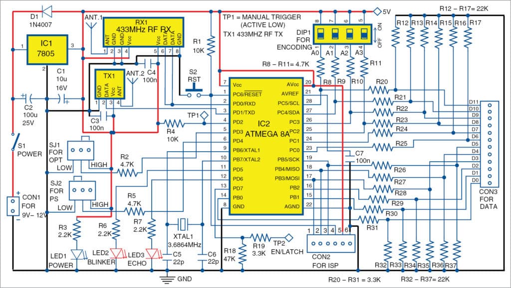
For conversion of 12-bit parallel data to serial data, and then of serial data to parallel data, ATmega8A MCU is used. It has inbuilt, separate serial data-out and serial data-in pins (USART). 12-bit parallel data is available digitally on the 12 pins of the MCU.
The circuit can be wired and used in two ways (modes) with slight modification, namely, transmission (TX) mode and receiving (RX) mode.
TX mode
If shorting jumper SJ2 is selected for high (5V), MCU is in transmission mode. The circuit can convert 12-bit parallel data (D0 to D11) available at connector CON3 to serial data and transmit it through its RF transmitter module TX1. RF receiver RX1 module is not required in this case.
RX mode
If SJ2 is selected for low (ground), MCU is in receiving mode. The circuit can receive serial data through RX1 and convert it to 12-bit parallel data (D0 to D11), which is available at CON3.
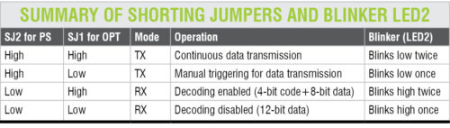
The same program is used for both transmitter and receiver sections. But for multiple functions, settings are done using SJ1 and SJ2. Option (OPT) selection is done using SJ1 to select encoding, or auto/manual transmission. Options are read by the MCU whenever it is powered up or reset by pressing reset (RST) switch S2. Program selection (PS) is done using SJ2.
SJ1 works differently with the combination of SJ2 selection as listed in the table (next page).
In TX mode, if SJ1 is high, continuous transmission happens at regular intervals. This is initially set in the program code (#define LOOP_DELAY 2000//milli seconds). If SJ1 is low, transmission is activated with falling edge on pin 4 (PD2) of MCU.
In RX mode, if SJ1 is high, decoding is active. And if SJ1 is low, decoding is inactive. Once decoding is active, the four MSB (D8 to D11) or address codes (A0 to A3) of receiver side should match the four MSB (D8 to D11) or address codes (A0 to A3) of transmitter side. Output data is available on D0 to D7 (8 bits only) of CON3.
Receiver side does not respond to the transmission signal if address codes or MSBs are mismatched. Four MSB codes and eight LSB data (total 12-bit data) are transmitted, and 16 such data sets can be transmitted from the transmitter unit without interference.
Blinker LED2 blinks once in RX mode without decoding and twice with it. It goes low once in TX mode with manual triggering and twice with continuous data transmission.
Echo LED3 blinks whenever data is transmitted or received. Output available at TP1 can be used for enabling/latching the new data available on D0-D11 pins, if required.
Manual triggering is low and can be applied at TP1. On receiving new data by receiver circuit, TP2 is active high for about 500 microseconds.
To understand decoding on receiver side, set SJ1 to high and connect a 4-way DIP switch. Then, set 4-bit (A0-A3) address on the DIP switch. Now, send data from TX side. RX side receives 8-bit data, if A0-A3 settings for both transmitter and receiver match; otherwise, 8-bit data is not received.
Software
The program (parallelserial.c) is written in C and compiled using AVR Studio4. After the circuit connections are done, write/burn parallelserial.hex file to ATmega8A MCU using a suitable AVR programmer through ISP port CON2.
There is no fuse-bit setting in the programmer. By default, low fuse bit is E1 and high fuse bit is D9. Fuse-bit settings for crystal are required if 3.6864MHz (XTAL1) crystal is connected, which is optional. Use the same crystal in both transmitter and receiver boards to achieve synchronisation of serial data transfer.
Download Source Folder
Construction and testing
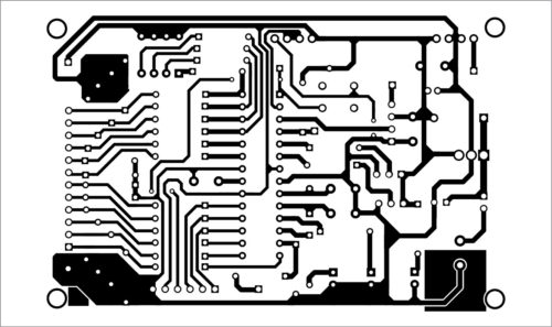
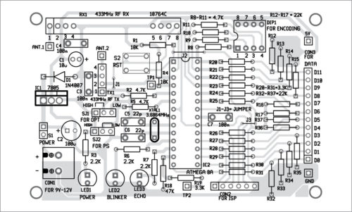
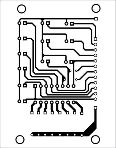
An actual-size PCB layout for the 12-bit signal transmitter and receiver is shown in Fig. 2 and its components layout in Fig. 3. Assemble two sets (boards) of the designed PCB: one for transmitter board with TX1 and another for receiver board with RX1. Note that, RX1 is not required in transmitter board and TX1 is not required in receiver board.
A separate DC power supply (9V-12V) is required for transmitter and receiver boards. Upload ParallelSerial.hex code to the respective MCUs of transmitter and receiver boards. Set transmitter board in TX mode with continuous data transmission by making SJ1 and SJ2 high. Set receiver board in RX mode without decoding by making SJ1 and SJ2 low.
Connect pin 3 of ATmega8A of transmitter board to pin 2 of ATmega8A of receiver board. Connect ground lines of both boards. Also, a data input-output (I/O) board can be connected temporarily to CON3 of transmitter and receiver boards for testing.
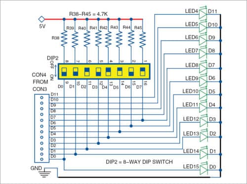
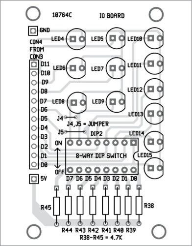
Circuit diagram of I/O board is shown in Fig. 4. PCB layout and components layout of the I/O board are shown in Figs 5 and 6, respectively.
Download PCB and Component Layout PDFs: click here
Now, switch on both the boards. LED2 indicates the status of the board setting, as shown in the table. Change address code A0-A3 and feed data input from transmitter side by randomly connecting some data pins (D0-D11) to 5V through DIP switch. Then, observe the output on the 12 LEDs on receiver board. The same data should reflect on the LEDs on the receiver side, if address codes A0-A3 of the receiver are the same as transmitter address codes.
Once testing is successfully done, remove I/O board connections from both the boards. Connect 433MHz RX1 with RX board and 433MHz TX1 with TX board. The boards can now be tested for decoding and manual triggering as per the table. After successful testing, the boards are ready to use.
Fayaz Hassan is manager at Visakhapatnam Steel Plant, Andhra Pradesh. He is interested in MCU projects, mechatronics and robotics.