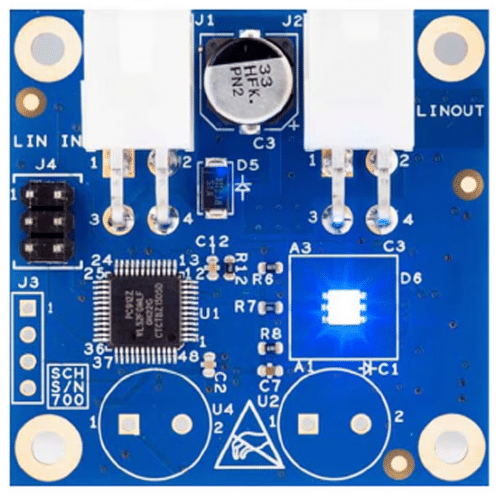
The board is designed for RGB LED control and diagnostics in automotive and industrial applications. It features a microcontroller and integrated high-voltage analogue components.

RGB LED lighting, which combines red, green, and blue to produce a broad spectrum of colours, is highly valued for its energy efficiency, versatility, and excellent colour control. This technology has revolutionised lighting applications across multiple sectors, from stage design and interior decorating to smart home systems and industrial uses. By offering dynamic colour changes and integration with IoT devices, RGB LEDs provide substantial energy savings, durability, and environmental benefits, making them a crucial development in modern lighting solutions. The S12ZVL32-LED is a reference design board developed by NXP semiconductors for controlling and diagnosing RGB LEDs via a local interconnect network (LIN).
The board utilises the 16-bit S12 MagniV S12ZVL mixed-signal microcontrollers and features an automotive voltage regulator, a LIN interface, a Vsup module for sensing automotive battery voltage, and an HVI pin. The platform delivers a cost-effective and highly integrated solution ideal for automotive LIN nodes where space is limited. This family offers memory options ranging from 8K to 128K flash, allowing for scalable platform standardisation.
The S12ZVL combines an advanced S12Z core with a 12 V to 5 V voltage regulator and a LIN physical layer transceiver, making it suitable for automotive and industrial applications, including sensor interfaces, actuators, switch panels, and ambient lighting.
The S12ZVL-family port integration module manages the connection between peripheral modules and the I/O pins across all ports. It oversees the electrical properties of the pins and handles signal prioritisation and multiplexing for shared pins.
The MC9S12ZVL Family comprises 16-bit automotive microcontrollers crafted using 180nm NVM + UHV technology, which allows the integration of 40V analogue components. This family incorporates several features from the existing S12 portfolio while distinguishing itself through an enhanced S12Z core and the inclusion of high-voltage analogue modules. The voltage regulator (VREG) and a Local Interconnect Network (LIN) physical layer are critical among these modules.
The background debug controller (BDC) is a single-wire, background debug system integrated into the on-chip hardware to minimise CPU intervention. It connects directly through the device’s BKGD pin. The S12ZBDC retains the traditional S12 serial interface protocol while introducing an advanced handshake protocol and an expanded BDC command set. This enhancement supports the linear instruction set unique to the S12Z device family and facilitates easier, more flexible access to internal resources via the BDC serial interface.
S12 devices offer various power modes, including run, wait, and stop, along with operating modes like normal and special single chips. Additionally, the functionality of the background debug controller (BDC) is contingent upon the device’s security status.
NXP has tested this reference design. It comes with a bill of materials (BOM), schematics, assembly drawing, printed circuit board (PCB) layout, and more. The company’s website has additional data about the reference design. To read more about this reference design, click here.


